Abstract
The goal of this project is to implement a XR-2206 based VCO with digital control of frequency, amplitude, wave shape, and duty cycle, maximizing the use of on-chip capabilities of the XR-2206.
This project may be used as a standalone function generator. A MCU is used for tuning of the aforementioned parameters. Hence, This is why it is said to be « digitally controlled » compared to manual potentiometer control.
The incentive for using an analog XR-2206 VCO instead of a simpler DDS (Direct Digital Synthesis) IC is to offer a solution that exploits the unique feature of the XR-2206, as waveform symmetry adjustment and THD control.
In some situations, injecting an analog signal with its artifacts may be of interest.
As an analog oscillator, the XR-2206 is free from digital aliasing artifacts.
It is also a good choice for musical instrumentation as an analog synthesizer, as it’s unique features (symmetry adjust / THD control / wave-shaping from sine-wave to triangle wave) give warmth to the generated sound, which is sought after in the analog synth market.
It also allow a faster development than a full-on discrete analog oscillator design.
Presentation of the XR-2206 IC
The XR-2206 is a VCO containing two sub-oscillators, with a keying pin allowing the selection of either sub-oscillator for output on two signal output pins, one presenting a sine/triangle/saw shape, the other pin being the output of a square wave signal.
Frequency Control
Current controlled
Coarse frequency control is achieved through the use of a given resistor to ground from the frequency current control pin. Each oscillator has its dedicated frequency control pin.
Frequency range (common to both oscillators) is further achieved through the use of a capacitor on the capacitor timing pins.
The resistors and capacitor are further referred as « timing resistors » and « timing capacitor ».
The resistor pins are further referred as timing current pins.
This basic frequency control achieved in this manner is dependent on the current flowing through the resistor timing pins, hence, this setup gives, strictly speaking, a current controlled oscillator for frequency selection.
The data sheet states the minimum value for the resistors being 1K, in order not to exceed the safe margin for current sourced from the timing pins.
The formula for the frequency of oscillation for each oscillator being 1/(R_subosc*C), C being the capacitance of the frequency range capacitor common to both oscillators.
The timing current pins are internally biased at +3V
A coarse MCU control of frequency can be achieved in this manner through the use of digital potentiometer wired as a rheostat.
Renesas X9C10x series were demonstrated to work well in this setup, as the voltage to ground is inside the specification range, When using X9C102, a trimming rheostat must be included so the current sourced from the pin does not exceed the safe specification margins of both the digital potentiometer and of the XR-2206. (values??)
A more granular current control scheme can be achieved by using the digital potentiometers X9C104, X9C103, and X9C102 as rheostat in series to ground to achieve at 10 ohm step.
However, this approach has drawbacks :
X9C10x series have up to 20 % tolerance in total R_High to R_Low values, although the resistance value of each R step on the R ladder demonstrates good linearity.
Thus, It is imperative to carefully select matched digital potentiometers for both sub-oscillators and measure precisely the resistance of each digital potentiometer so that the MCU can tune the frequency with minimum readjustments.
Also, the use of multiple digital potentiometers in series makes the frequency tuning control algorithms more complex and each new potentiometer introduces error coming from the resistance measure and makes the time to tune longer. Careful design must be implemented so that out of tuning bounds events for each potentiometer do not happen, which would further delay the time to tune.
For all these reasons, a single digital potentiometer in rheostat mode for coarse tuning plus a DAC chip in voltage control mode for fine tuning is preferred as it reduces the number of digital control channels, while maintaining a large frequency range and good frequency resolution, while minimizing tuning time, but increasing BOM costs.
Nevertheless, if tuning time is not a priority, a lower cost hardware setup with higher control complexity algorithm can be devised.
Example of operation for an audio range frequency current control setup with three X9C10x digital potentiometer in series at each R timing pin.
In this setup, a polypropylene capacitor of 0.044 µF is inserted on the frequency range capacitor pins.
Provided that a trimming potentiometer in rheostat mode, is inserted in the series with one X9C104, one X9C103, and one X9C102 digital potentiometer in series, the minimum R_trim value setting the highest achievable frequency will be set so that the lumped resistance is no less than 1KΩ, stated by the XR-2206 datasheet as the minimum resistance for safe operation.
Additionally, the XR-2206 datasheet shows exponential degradation of frequency stability at large (>200 kΩ) and low (~1kΩ) timing resistors values. Thus, it is not advisable to use digital potentiometers with a total lumped resistance above 200 kΩ. This is the primary factor restricting the range of output frequencies.
Obtaining several output range frequencies can be done by selecting different capacitors of a bank in 1 of n fashion.
The X9C10x series was selected for its low cost, up to 7V voltage maximum rating and current rating in the low mA range. It also features recall of last setting at power-up, if needed, with a durability of 100000 cycles per bit of the recall logic.
However, it does not offer logic query of the current setting. That means that the MCU should maintain the potentiometer states in RAM and EEPROM if a recall of the setting at power-up is required. However, in-board MCU also have a cycle write limit for EEPROM, thus a flash memory storage would be preferable for frequent updates.
In the case of a musical instrument, the settings of these potentiometers affect frequency only, not timbre, and thus can be discarded at power-off.
Determination of frequency range
On the X9C10x datasheet, it is stated that the minimum resistance of the digital potentiometer is 40Ω, corresponding to the wiper resistance, noted RwiperR_wiperin the following formula defining the minimum value of the trimming resistance based on three digital potentiometers in rheostat mode used in series :
3∗Rwiper+Rtrim>1kΩ3*R_wiper + R_trim > 1k %OMEGA
solving for RtrimR_trim, supposing RwiperR_wiper being close to the nominal 40 Ohms value.
Rtrim>880ΩR_trim > 880 %OMEGA
And, with C set at 6.6e-8 F (0.066 µF),
We can compute the maximum frequency we can obtain :
fmax=11000∗6.6E−8f_max = {1} over {1000 * 6.6E^-8}
fmax=15151Hzf_max = 15151 Hz
The lowest achievable frequency, provided that the potentiometers are each at nominal values of, respectively, 100 kΩ, 10 kΩ and 1 kΩ, and set at RmaxR_max, so that Rmaxtotal=100k+10k+1k+880+3∗40R_maxtotal = 100k + 10k + 1k +880 + 3*40 :
Rmaxtotal=112kΩR_maxtotal = 112k %OMEGA
fmin=1112E3∗6.6E−8f_min = {1} over {112E^3 * 6.6E^-8}
fmin=135.8Hzf_min = 135.8 Hz
In the following implementation of a VCO for a musical application, as a synthesizer, RtrimR_trimwas offset at a higher value so that :
fmin=f(C3)=130.8Hzf_min = f( C3 ) = 130.8 HzThe three digital potentiometers being set at full-scale (99,99,99)
Based on the aforementioned relation, We can solve for RtrimR_trimand RmaxtotalR_maxtotal
So that,
Rmax=115,84kΩR_max = 115,84 k %OMEGA
Rtrim=4.717kΩR_trim = 4.717 k %OMEGA
Note that by doing this, fmaxf_max is then offset to a lower value of 3132 Hz.
Which gives us a frequency range close to 4.5 octaves. (C3 to F#7)
Frequency tuning step resolution
Since the three digital potentiometers have 100 equal R steps (from 0/99*r_max to 99/99*r_max) and are fully overlapped, in the sense that no R setting is not accessible int the [Rmintotal,Rmaxtotal][R_mintotal , R_maxtotal], the RstepR_step of the lowest resistance digital potentiometer (X9C102) gives the resistance step resolution, that is,
Rstep=1E399R_step = {1E^3} over {99}
Rstep=10.1ΩR_step = 10.1 %OMEGA
Which gives a frequency resolution at fminf_min of :
Δfmin=1(115.84E3−10.1)∗6.6E−8−1(115.84E3)∗6.6E−8%DELTA f_min = {1} over {(115.84E^3 - 10.1)*6.6E^-8} - {1} over {(115.84E^3)*6.6E^-8}
Δfmin=0.0114Hz%DELTA f_min = 0.0114 Hz
and at fmaxf_max:
Δfmax=1(4.837E3−10.1)∗6.6E−8−1(4.837E3)∗6.6E−8%DELTA f_max = {1} over {(4.837E^3 - 10.1)*6.6E^-8} - {1} over {(4.837E^3)*6.6E^-8}
Δfmin=6.5544Hz%DELTA f_min = 6.5544 Hz
In terms of musical units, the interval compared to C3 at fminf_min is :
Δfmincents=1200∗log2(f(C3)+Δfminf(C3))%DELTA f_mincents = 1200*log2({f(C3) + %DELTA f_min} over {f(C3)} )
Δfmincents=0.1508cents%DELTA f_mincents = 0.1508 cents
And at f_max = 3132 Hz
Δfmaxcents=1200∗log2(3132+Δfmax3132)%DELTA f_maxcents = 1200*log2({3132 + %DELTA f_max} over {3132})
Δfmaxcents=3.619cents%DELTA f_maxcents = 3.619 cents
Dynamic Tuning Algorithm
Single Sub-oscillator tuning
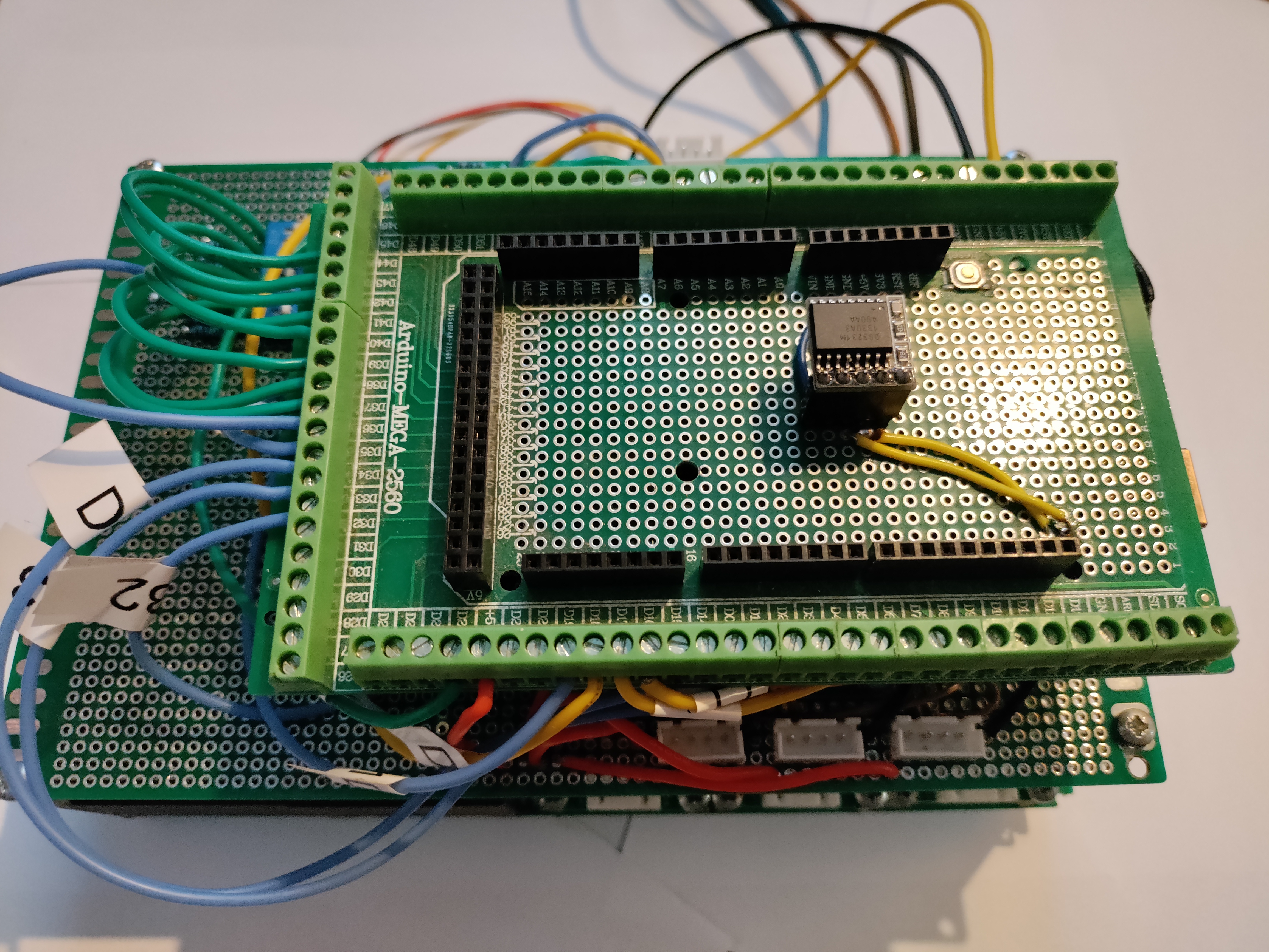
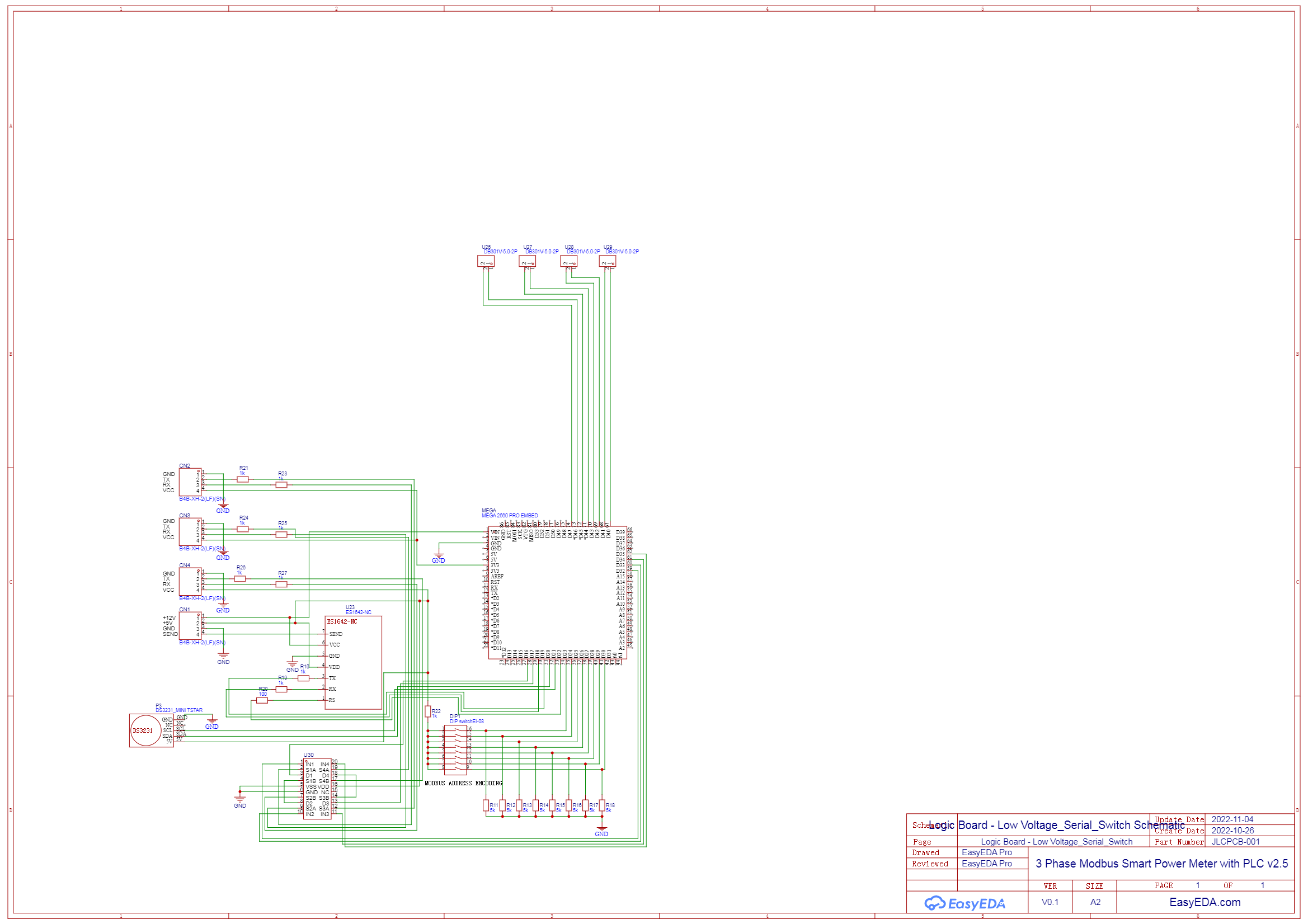
A fully digital algorithm based on the Arduino Mega 2560 was devised.
Measuring the frequency was achieved through the improved resolution timer2 library and a modified version of the PulseIn that integrates the 0.5µs precise timer2 library instead of the 4µs standard precision.
It should be noted that accurate frequency measurements are dependent on the clock frequency of the Arduino. Arduino mega 2560 is clocked at 16 Mhz, However it uses a ceramic oscillator instead of Quartz crystal oscillator. Thus, it is probable that the oscillation is not an exact 16 Mhz.
This is not a problem for interval tuning since it is based on frequency ratios, but may introduce de-tuning if the synthesizer signal is to be integrated into an ensemble of other instruments using, for instance, a reference tuning of A4 = 440 Hz.
Also, The higher the working clock frequency of the MCU, the higher is the measure resolution. and tuning speed. However, the limiting factor in the tuning speed achieved is the period of the signal. Measuring the frequency is usually done through signal level or edge triggering or zero cross method, all requiring at least a lapse of time of 1/f_fundamental to compute the frequency of the signal.
In practice, oscillator drift, noise, may require averaging several frequency measurements to obtain a reliable measure.
In this implementation, the number of frequency measure sample has been set to 10.
An analysis of the statistical distribution of frequency measures over a medium interval (like 10s) will give an idea of the effects of noise, digital aliasing artifacts. Oscillator drift is usually temperature dependent and should be minimized by using an adequate capacitor with a flat temperature to capacitance response. (temperature drift compensating)
In this implementation, low ESR metalized polypropylene capacitors are used, for their adequate frequency response, long lifetime and parameter stability over time.
The first step in tuning uses the f = 1/RC formula, solved for R. It is important to have a precise measure of the timing capacitor capacitance at standard temperature conditions of use.
R = 1/fC.
Now, three values of resistance should be determined satisfying the following conditions :
R1 + R2 + R3 = R – Rtrim - Rwipers
R1 < 100K
R2 < 10K
R3 < 1K
Ideally, R2 and R3 values should be as close as possible to the mid-range of the digital potentiometer, that is, 10K/2 and 1K/2. This gives leeway for fine tuning of R2 and R3 in both increasing and decreasing R steps.
Based on the above formula, the three digital potentiometers are set to their respective values, and the sub-oscillator frequency is measured.
The frequency error is then : ferror=ftuned–fmeasuredf_error = f_tuned – f_measured
The goal being to tune the oscillator at the R value of min(|ferror|)min(abs{f_error})
A standard gradient descent approach based on the derivative of frequency over resistance function is used dRdf=−1f2∗C{dR} over {df} = {-1} over {f^2 *C} so that the step delta_R for each R correction is given by :
ΔR≃−1f2∗C∗ferror%DELTA R simeq {-1} over {f^2 *C} * f_error
In practice, a tuning factor k is introduced and determined empirically in case of undershoots /overshoots, k < 1 in case of overshoots and k > 1 in case of undershoots
ΔR≃−1f2∗C∗ferror∗k%DELTA R simeq {-1} over {f^2 *C} * f_error * k
Considering a simple algorithm that would make corrections on the digital potentiometer R values sequentially, starting with the highest value potentiometer for coarse tuning. The potentiometer step change number is given by the rounding to the nearest integer function [❑][<?>] :
ΔRsteps=[ΔRRpotstep]%DELTA R_steps = [ {%DELTA R} over {R_potstep} ]
being the value in ohms of the digital potentiometer under consideration
For each potentiometer, a ΔRsteps%DELTA R_stepstuning deflection is applied and ferrorf_erroris sampled. Depending on the tuning factor k, the following conditions will arise.
For a sub-optimal too low k, the series made of each step ferrorf_error will converge to 0 without sign change, the less optimal the k, the more steps before reaching the condition :
ΔR<Rpotstep{%DELTA R} < {R_potstep}
For a sub-optimal too high k, the series made of each step ferrorf_error will converge to 0 with zero crossings at each tuning step , the less optimal the k, the more steps before reaching the condition :
ΔR<Rpotstep{%DELTA R} < {R_potstep}
It may be useful to have a slightly sub-optimal too high k, so that a zero-crossing for ferrorf_errorcondition is achieved faster after a last tuning step of exactly1Rpotstep1 R_potstep
So that min(|f(error(n−1))|,|f(error(n))|)min(abs{f_(error(n-1))}, abs{f_(error(n))})decides if the last tuning step is discarded or conserved.
However, The smallest potentiometers current settings should be taken into account before selecting the higher value potentiometer setting such that an out of tuning bound condition may not arise.
The process is repeated for the smaller potentiometers until the ferror<ferrorthresholdf_error < f_errorthresholdcondition arises.
In this implementation, ferrorthresholdf_errorthreshold was set at ± 2 musical cents.
The tuning algorithm speed is a function of the number of tuning steps times the tuning time per step. The tuning time per step if made from computational overhead and most significatively, the time it takes to measure the signal frequency times the number of frequency measure samples.
ttuning=nsteps∗(nsamples∗(tperiod+tcompmeas)+tcomptuning)t_tuning = n_steps * (n_samples * (t_period + t_compmeas) + t_comptuning)
n_steps can be optimized as already discussed above by fine tuning k and by a precise measure of C and RmaxR_maxand by selecting a proper capacitor (metalized polypropylene film is a good choice and metal film resistors with low inductance parasitics, although these considerations are of prime importance in higher frequency ranges only, less in audio, except for the capacitor regarding temperature dependency), so that the circuit deviates as less as possible from 1/RC law.
Algorithmically, n_steps can also be reducing by stepping all required digital potentiometers at each
step instead of stepping them sequentially, as it will be described in the optimized algorithm in the next section.
nsamplesn_samples can be optimized by analyzing the statistical distribution of frequency measures, as it will impact the precision of the obtained frequency, taking into account a goal of 2 cents in our application, note that the smallest time component that can be measured for a single suboscillator is :
thalf=12∗ft_half = {1} over {2*f}as it is the time interval returned by either PulseIn(LOW) or PulseIn(HIGH) for a 0.5 duty cycle signal. Thus the tuning time will be strongly dependent and inversely proportional to the frequency. Reducing noise by using proper circuit design and adequate low pass filtering on the measuring frequency pin is of prime importance.
The worst case tuning speed obtained was close to 1.5 seconds (fr C#3) and close to 0.4 seconds at high frequencies (B#6). Using the naive sequential digital potentiometer tuning method described above.
tcompmeast_compmeas is very light in computing time, and generally only decreases the frequency measure resolution, because that overhead is compounded into the frequency measure value. Using a faster Arduino MCU (like The Due) with a precise XTAL Quartz oscillator and a precise Timer library will improve measuring precision and resolution substantially.
tcomptuningt_comptuning can be minimized by applying general Arduino coding best practices, using extra care on the computational intensive parts of the algorithm.
For all these reasons, a debugging mode with timing display should be used to quantify performance gains and overall tuning duration performance.
Optimized parallel tuning algorithms
If the deviation from theory is small, the overall delta R may be sufficiently small from the theoretical value that only the lowest R digital potentiometer is stepped to obtain accurate frequency
In other cases, if the deviation requires a tuning step above the highest digital potentiometer R step,
A parallel tuning may be experimented with and compared to the sequential tuning in term of performance. This may work well if each potentiometer has good step linearity and each potentiometer R value is measured precisely.
Note that for the theoretical determination of each potentiometer step, it is good practice, if the R value make it possible, to bias the medium and low value digital potentiometer at half scale, so it gives leeway for up and down stepping. (~5k for X9C103 and ~0.5k for X9C102)
Then, the delta R, once computed, should be distributed across the potentiometers. Since the potentiometers are overlapping, there is more than one way to distribute delta R across them.
The selected way should avoid if possible to step potentiometers close to their stepping bounds. (0 , 99)
Consider the following example to illustrate the algorithm :
Tuning for f(A4) = 440 Hz,
We have, R=1440∗6.6E-8R = {1} over {440*6.6E-8}
R = 34 435 Ω
Let’s first take R_trim out including wiper resistances :
R_pot = 34435 – 4.8237
R_pot =29 608
Now let’s bias the medium and low potentiometers to ~5K and ~0.5K (Supposing that they were chosen to have nominal values).
R_pot_remaining = 29608 – (49/99)*10000 – (49/99)*1000 = 24163 Ω
Let’s perform the division of that value by the highest pot R step and half-step round to the closest integer.
24163 / (100 000/99) = 23.92137
In that case, we will select the R step at 24.
That means that the reminder will be negative, and thus subtracted from the biased medium/low pots.
The reminder being 24163 – 24*(100 000/99) = -79.42 Ohms.
Now we have to distribute the reminder across the X9C103 and X9C102 pots.
Let’s repeat the division scheme
-79.42 / (10 000/99) = - 0.7862
In that case we select a step of -1.
The reminder being -79.42 - (-1*(10 000/99)) = 21.59 The reminder is once again positive, since we overcompensated.
Let’s do it one last time/
21.59 / (1000/99) = 2.13741
21.59 \ (1000/99) = 2 and the remainder is 1.38
Now let’s add these values to the potentiometer initial biasing.
XC9103 steps = 49 - 1 = 48
X9C102 steps = 49 + 2 = 51
Let’s recheck the R obtained :
24*(100 000/99) + 48 *(10 000/99) + 51 * (1000/99) = 29606.06 (~29608 being the R value above that we approximated)
Compound oscillator with arbitrary pulse width tuning
For a given fundamental frequency and duty_cycle, the two sub-oscillator requested frequencies are determined from theory and their corresponding potentiometer settings.
Since The Arduino PulseIn can discriminate between LOW levels and HIGH levels, the frequency of individual sub-oscillator can be measured from the compound signal, in self-keying mode, without the need to toggle the FSK pin.
f_subosc = 1/(2*t_level)
We did not observe 180° phase reversals of the compound signal in our setup, which would also switch duty cycle between duty and 1 – duty, Which is good since it makes identification of the tuned sub-oscillator easier.
The tuning method used above would tune the sub-oscillator with the highest frequency first. Using PulseIn (LOW / HIGH) the sub-oscillator frequency is extracted and tuned.
Then, the sub-oscillator with the lowest frequency component would then be fine tuned taking into account the fundamental frequency of the compound signal.
Using the frequency component of the remaining sub-oscillator instead of the compound signal fundamental frequency for the last step of tuning yields substantial error in our setup. Thus it is avoided and instead the fundamental frequency is used in the last sub-oscillator tuning step.
The detrimental effect this method has is that it introduces error in the duty cycle setting. However it is less critical than an error in the fundamental frequency.
Static Tuning Algorithm
If the circuit under consideration exhibits deviations from theory or a precise measure of the components could not be achieved, and the tuning time is deemed unacceptably high, as it may be the case for a musical instrument where the fundamental frequency must be set at once, it is possible to use the above tuning algorithm and store the potentiometer values determined for a set of discrete frequencies in EEPROM of flash.
While the number of entries in the lookup table is reduced for a single sub-oscillator (usually 12 notes per octave), The number of entries is greatly increased in the case of a compound oscillator based on the two sub-oscillator (for pulse widths different from 0.5).
The number of entries will then directly influence the fundamental frequency resolution and/or the duty cycle resolution.
Lookup Table memory footprint
Each digital potentiometer has a 100 step resolution. A byte memory variable can then store 2 digital potentiometer settings. Each sub-oscillator uses 3 digital potentiometers. For a given frequency, the settings of the two sub-oscilllators can be stored using 3 bytes.
A two cents separation lookup table for frequencies from C3 to C7 would then store 48*50 = 2400 intervals.
Such an optimized lookup table would use 7200 bytes of memory. These values would not need to be changed at run-time so burning them in the Arduino Mega flash (256KB) is adequate.
Compound oscillator tuning based on lookup tables.
As for the dynamic tuning, The two sub-oscillator frequencies are computed from a given waveform with frequency and duty cycle parameters.
The closest frequency settings of the digital potentiometers are then extracted from the lookup tables.
By using interpolation of two adjacent potentiometer settings, further precision of the tuning can be achieved.
The downside of the static tuning method is the length of time it takes to create the initial tuning map, (or whenever a timing digital potentiometer, capacitor, or XR-2206 chip is replaced) and eventual deviation in case of poor component stability with time.
Thus, it is preferred to have both methods at hand and use one or the other, or a combination of both depending on the situation.
It should be noted too that the X9C10x digital potentiometers are resilient but simple devices. They are increment/decrement step based devices with last set value recalled at power-up. The current setting however, cannot be queried. It is then compulsory to store the current setting in RAM to track the current value of the potentiometer by integrating all step changes during the power cycle and taking care not to step out of the setting bounds.
A multiple hour operation however has not shown any discrepancies between the in RAM setting and the potentiometer R value. Noise or power supply issues could cause the potentiometer to skip a commanded change, but it was not observed in our breadboard prototype.
For good measure, an out of bounds increase/decrease command can be sent with an increase or decrease value greater than the number of steps to reset the potentiometer to its lower or upper bound.
In the case of a musical synthesizer, this should be done when the VCA is at rest, so no artifact sound is played.
Voltage Controlled operation
The XR-2206 can be controlled by a voltage input ranging from 0 to 3V, in the following manner, as per the datasheet :
The voltage to frequency formula is then :
f=1RC(1+RRC(1−VC3))f = {1} over {RC} ( 1 + {R} over { R_{C}} (1 - {V_{C}} over {3} ) )
In this setup, the sweep input is connected to the output pin of a voltage DAC. The output stage of the DAC must be able to sink current.
The voltage range of the DAC will be restricted to [0, 3V]
For safe and reliable operation, We have to size RCR_C and R so that It⩽3mA I_{t} leslant 3mA
If VCV_C is set at 0V, ItI_twill be :
3∗R∗RCR+RC<3mA3 * {R*R_C} over {R + R_C} < 3mA
Supposing for design simplicity that RCR_Cis a fixed lumped resistance and that R is variable and that RC≥RminR_C >= R_min
It follows that R and RCR_C should be sized to at least 2 kΩ
Note that the DAC output impedance stage should be taken into account for RCR_C
Considering RCR_Cand C fixed, the frequency setting is obtained through R and VCV_C
We have now to degrees of freedom to set the frequency.
We will first ensure that the obtain frequency range in this setup goes at least from C3 to C7
The principle of operation in this setup uses VCV_C voltage in the [0, 3V] range, for fine tuning of the frequency, with a resolution dependent on the bit resolution of the DAC
R, as a digital potentiometer in rheostat mode, for coarse fine tuning. A too small R digital potentiometer would severely restrict the frequency range. So, we should consider first the highest R value digital potentiometer, the X9C104 of RmaxR_max = 100k Ω
Since in this setup we are using a single X9C104, And since we will also make use of a trimming resistor RtrimR_trimso that At RmaxR_max f=f(C3)f = f( C3 ), by increasing RtrimR_trim to compensate for the removal of the X9C103 and the X9C102, thus adding 11 kΩ , we may not reach C7 at RminR_min
Indeed, with RtrimR_trim = 15.827 kΩ, at Rmin=RtrimR_min = R_trim, f=115.827E3∗6.6E−8=967.32Hzf = {1} over {15.827E^3*6.6E^-8} = 967.32 Hz
That is well under our target of at least 2093 Hz.
However, if we carefully select a X9C104 in high portion of the tolerance range of the manufacturer specifications ( ± 20%), This would decrease the required R_trim value.
In our component survey of over thirty X9C104 chips we found five with a RmaxR_maxvalue of over 110kΩ
So, For a total RmaxtotalR_maxtotal of 114.827 kΩ and a X9C104 RmaxR_max of 110 kΩ, RtrimR_trim = 4.827 kΩ, which gives a maximum frequency with VCV_C= 3V, of :
f=14.827E3∗6.6E−8=3138.9Hzf = {1} over {4.827E^3*6.6E^-8} = 3138.9 Hzwell above C7, which is good.
We should then check that frequency control usingVCV_C and R, in the above defined frequency range is fully overlapping and thus encompasses fine tuning over the range C3 to C7.
Provided that the output stage of the DAC is scaled down through a less than unity non inverting OpAmp so that the n bits resolution is applied to the range [0 , 3V]
Assuming a 12bit DAC with it’s output range restricted to [0, 3V] through a voltage divider or better, an OpAmp with less than unity gain to keep output impedance low :
dVC=3212=0.732mVdV_C = {3} over {2^{12}} = 0.732 mV
Given the voltage to conversion gain formula, δfδVc=−0.32Rc∗C{ %delta f } over {%delta V_c} = {-0.32} over {R_c * C} Hz/V
We have to set Rc so that each voltage step has a frequency gain under 2 cents at C3, according to the following relation :
ferrorcents=1200∗log2(f(C3)+fstepf(C3))<2centsf_errorcents = 1200*log2({f(C3) + f_step} over {f(C3)} ) < 2 cents
Solving for step, step < 0.16021 Hz
With unitary voltage step of 3/2^12 = 0.732 mV
And the voltage to frequency gain, δfδVc=−0.32RC∗6.6E-8{ %delta f } over {%delta V_c} = {-0.32} over {R_C * 6.6E-8} Hz/V
δfδVc=−0.32RC∗6.6E-8∗0.732E-3=0.16021Hz{ %delta f } over {%delta V_c} = {-0.32} over {R_C * 6.6E-8} * 0.732E-3 = 0.16021 Hz
for a step of 0.732 mV, that gives a minimum Rc of 22152 Ohms
And a maximum frequency deflection over the 3V range of
δfδVc=−0.3222152∗6.6E-8∗3=−656Hz{ %delta f } over {%delta V_c} = {-0.32} over {22152 * 6.6E-8} * 3 = -656 Hz
At VCV_C = 3V, The formula reverts to the form 1RC{1} over {RC} with its derivative being
δfδR=−1R2∗6.6E-8Hz/ohm{ %delta f } over {%delta R} = {-1} over {R^2 *6.6E-8} Hz/ohmat R so that f = f(B6), R= 7671 ohm, We have a slope of -0.2574 Hz/ohm, for a step of 1.1Kohm (based on a X9C104 select with RmaxR_max= 110K), we have 283.14 Hz/RstepHz/R_step
This is under the 656 Hz total voltage deflection, So frequency control based on VCV_C in the [0,3V] and RstepR_step = 1.1kOhm is overlapping at the high end of the frequency range.
The upper bound for RCR_Cis given by the relation
δfδVc=−0.32Rc∗6.6E-8∗3>−283.14Hz{ %delta f } over {%delta V_c} = {-0.32} over {Rc * 6.6E-8} * 3 > -283.14 Hz
Which give a maximum value for RCR_C of 51371 Ohms.
Thus the allowable range for RCR_Cis :
22152 Ohms < RCR_C < 51371 Ohms.
In practice, fine tuning precision is more important than fine tuning range once overlapping tuning is guaranteed. Thus it is preferable to bias RCR_C toward the upper part of the [22152, 51371 Ohms] range.
However, taking advantage of higher precision fine tuning requires to invest more on the MCU (higher clock speed and calibration).
Reminder : Worst case scenario precision is 4µS on a AtMEGA2560
On the other hand, tuning ranges with larger depths may have their use for pronounced glide/vibrato effects. And having a large tuning range gives a higher probability of tuning at ± half semi-tone of the desired frequency based on voltage control alone. That depends however for each note at how close the fundamental is tuned to half voltage deflection (VCV_C = 1.5V).
If the ± half semi-tone glide exceeds the DAC range because of initial deviation from the 1.5V VCV_C center position, A step up/down of the digital potentiometer is required, which would induce an audible discontinuity in the vibrato / glide effect.
This is one fundamental issue of having a tuning method based on two discrete components (a digital potentiometer and a DAC), but is less pronounced that having the tuning relying on three digital potentiometers alone.
Tuning algorithm based on DAC + single X9C104 digital potentiometer.
This algorithm is intended to be simple and fast.
First, coarse tuning should be done at VCV_C = 3V so that the frequency formula reverts to the classic 1RC{1} over {RC} form.
A lookup table consisting of the obtained frequencies of the 100 steps of the X9C104 potentiometer could be populated if it happens that there is a deviation in obtained frequencies from the 1RC{1} over {RC} form. All things considered, the small footprint of the lookup table make it easy and fast to populate, so even if the gain in MCU computing time is marginal, it costs little to use one.
Since the voltage to frequency gain is negative, lowering the DAC voltage from its 3V rest point results in an increase in frequency.
Then, for a given arbitrary frequency, the digital potentiometer should be set at the setting level that result in a frequency immediately under the desired frequency.
And then, the voltage lowered according to the voltage to frequency gain formula to obtain the positive ferrorf_error deflection.
Compound oscillator with variable pulse width tuning
The algorithm is similar to the string of digital potentiometers in series algorithm , in the sense that the sub-oscillator with the highest frequency component is tuned first using PulseIn (LOW or HIGH)
using the digital potentiometer for coarse tuning and the VCO voltage gain formula for the fine tune step.
The remaining oscillator is then tuned to the frequency immediately under the desired frequency.
Using the voltage to frequency gain formula, When measuring the error on the resulting signal ferrorf_error, the frequency error on the component sub-oscillator signal fcmperrorf_cmperror is adjusted to
fcmperror=ferror2∗duty,whenduty>0.5f_cmperror = {f_error} over {2*duty} , when duty >0.5
or,
fcmperror=ferror2∗(1−duty),whenduty<0.5f_cmperror = {f_error} over {2*(1 -duty)} , when duty <0.5
Since we are tuning the lowest frequency component last.
Appendix A :
Duty Cycle control (SAW signal generation and SQUARE pulse width control)
Duty cycle / pulse width control is achieved through self-keying between the two sub-oscillators by routing the square wave pin output (SYNC0) to the keying (FSK) pin.
The FSK pin is level triggered (1V 3V) and selects sub-oscillator 1 or sub-oscillator 2. When self-keyed from SYNC0, The output is adjusted for phase in the following manner.
SYNC0 level is high when the TRI/SAW signal rises.
SYNC0 level is low when the TRI/SAW signal falls.
When FSK pin is triggered high, the output signal switches to sub-oscillator 2, with phase at Vmin, and the TRI/SAW signal rises, SYNC0 level stays high. The sub-oscillator 2 rising edge duration is
trise=12∗fsubosc2t_rise = {1} over {2*f_subosc2}
When sub-oscillator 2 reverts to the falling edge, SYNC0 level goes down and sub-oscillator 1 is selected, with phase positioned at VmaxV_max. SYNC0 level stays low. The sub-oscillator 1 falling edge duration is :
tfall=12∗fsubosc1t_fall = {1} over {2*f_subosc1}
When self keyed, the signal fundamental frequency at output pins is :
ffundamental=1trise+tfallf_fundamental = {1} over {t_rise + t_fall}
and the duty cycle is :
duty=trise(trise+tfall)duty = {t_rise} over {(t_rise + t_fall)}


)