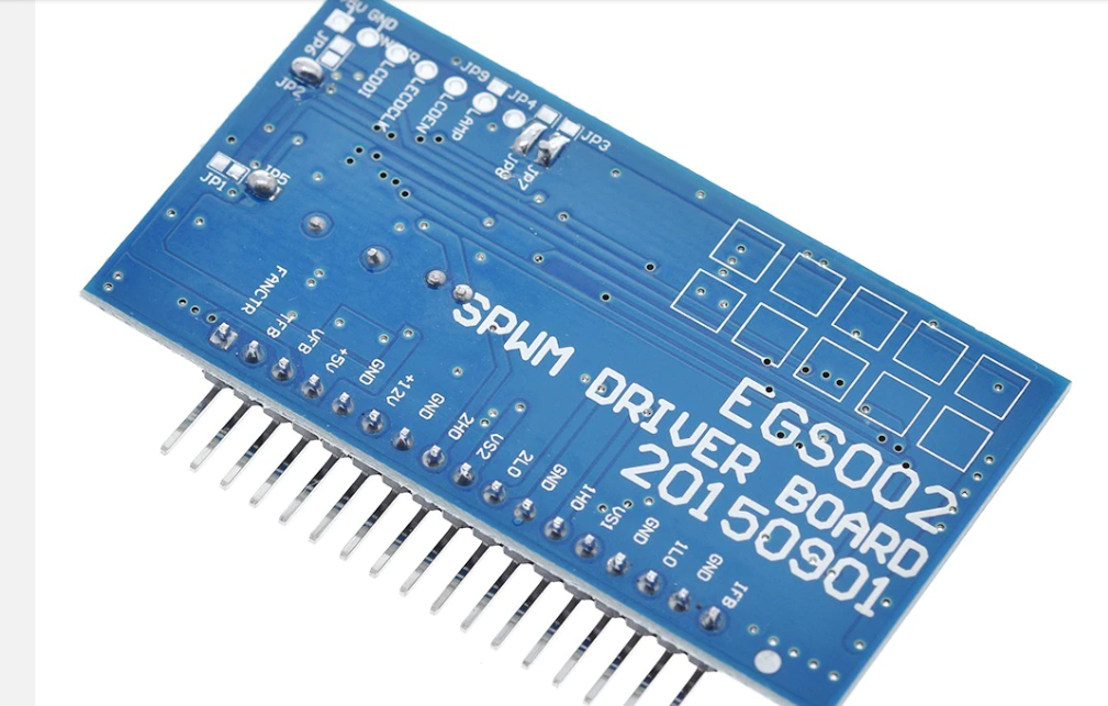
EGMicro EGS002 board review
The goal of this post is to analyze in detail the advertised features of the EGS002 board, and show possible modding hacks.
The EGS002 board is the oldest provided by the EGMicro supplier still distributed on common Chinese reseller platforms. It superseded the even older EGS001.
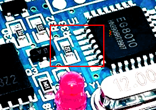
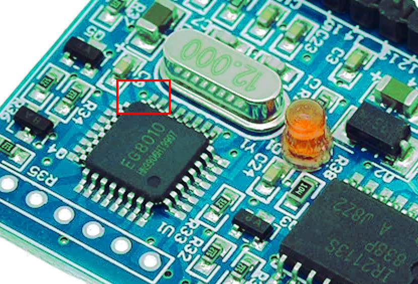
It is based on the EG8010 ASIC and also features either two IR2110S half bridge drivers, or two EG2113, an EGMicro driver. Whether you get one or the other depends on the reseller. Check for comments and reviews on marketplace product page to see who’s getting what.
Most if not all all of the EGS002 information is also provided in the EG8010 datasheet, plus many more details! We will use the EG8010 datasheet as the reference material, but also compare them to the EGS002 board features, to see what features are restricted by the board.
EG8010 ASIC Features
Input DC Voltage. The EGS002 can drive high voltage MOSFETs easily. no restrictive voltage limitations on the high side MOSFETs, and it is at least ok for 400V DC input to the MOSFET bridge. Supplied design schematics show power coming through a 400V DC link PFC output.
Inverter output frequency. EG8010 can be used for fixed 50Hz,60Hz or frequency adjustable 0~100Hz or 0~400Hz output.
The EGS002 on the other hand restricts this feature to fixed frequency operation : either 50Hz or 60Hz, through jumpers.
These jumpers are exposed on the bottom plane of the board and are set with solder bridges over two pads. They do not appear to be through hole, so it would be difficult to insert header pins and use a real jumper there.
JP1 and JP5 on the board control FREQSEL0 pin 18 level (either HIGH=JP1 short for 60Hz or LOW=JP5 short for 50Hz). They can’t be short or open at the same time !!
Is the board moddable for further frequency control ? let’s see.
There seems to be two methods to apply mods. Either through hardware or through software (by serial commands). Let’s explore the hardware method first.
Variable Frequency mode modification
Up to 100Hz or up to 400Hz variable frequency operation mode selection is controlled by FREQSEL1. It seems however that the EGS002 has the FREQSEL1 pin 19 grounded in the EGS002 schematic. So it depends on the suppliers of EGS002 to create derivative boards that expose FREQSEL1.
As far as I searched on Chinese marketplaces that doesn’t seem to be the case.
FREQSEL1 pin 19 and MODSEL pin 20. seem both connected to ground in most boards available on the market through merging traces. This is in conformity with the EGS002 datasheet.
That restricts the unmodded board to 50/60 Hz Operation and Unipolar switching
Modding for tests to enable VVVF to 100 Hz or to 400 Hz would require cutting the FREQSEL1 pin trace and patching the pin with maybe AWG30 hookup wires and connect it to HIGH level. MODSEL would be still kept to GND.
JP1 and JP5 would allow to control max frequency to 100Hz or 400Hz.
Note that variable frequency with constant voltage mode and variable frequency with variable voltage both require Unipolar switching. That is why you don’t have to bother with MODSEL in this mod
Once FREQSEL1 is set to HIGH, Variable frequency mode type is enabled through VVVF pin 32. In EGS002 again, it is connected to ground. This mode would give EGS002 the variable frequency constant voltage mode by default. (without further mods)
To enable VVVF variable freq/variable voltage (albeit with constant V/F ratio) for single phase VFD applications, bring VVVF to HIGH
Again, the trace after the pin may be cut if other pins do not depend on the cut trace, which may be difficult to check since some trace may hide under the IC.
Note that there are several test points / open vias on the board that can be used to patch the board with additional connections.
Then you have to expose FRQADJ/VFB2 pin to set the desired frequency in variable frequency mode through an external potentiometer in figure 8.6a of the datasheet. Voltage regulation is still performed through R23 and VFB1
In constant voltage/frequency ratio mode, you use R23 to set the nominal voltage at 50Hz through VFB1 Frequency ratio control goes through FRQADJ/VFB2 in this mode. It is a bit unclear in the datasheet.
Bipolar SPWM enable modification
Remember that you cannot use VVVF features in this mode.
The mod would require :
- cutting MODSEL pin 20 trace to disconnect from ground and patch it logic HIGH.
- cutting FRQADJ/VFB2 pin 16 trace/pad to disconnect it from ground and use it to supply voltage feedback as shown in the EG8010 bipolar switching application schematic. In this mode VFB pin 13 and FRQADJ/VFB2 pin 16 are supplied a differential voltage feedback. It is required in bipolar switching. .
However, all boards found on the market seem to implement the application schematic “Figure 6‐2. EG8010+IR2110S+cross‐conduction prevention logic sinusoid inverter(unipolar modulation)”
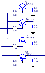
The cross conduction prevention logic is inserted between the ASIC logic outputs and the Gate drivers logic inputs. It consists of resistors and BJTs
I think that would prevent the bipolar SPWM mode from working. So you need further modding.
- You need to unsolder Q2 Q3 Q4 Q5 and solder bridge collector and emitter pads.
- Remove resistors R30 to R37
Using the UART to set the operation modes
The ASIC also exposes an USART interface (RX pin 4 and TX pin 5)
The data inteface looks powerful, exposing all configuration options usually set by the jumpers. Whether the override of the jumpers is properly done by the USART remains to be seen.
Note than enabling bipolar SPWM would still require the removal of the cross conduction prevention components.
It also allows for monitoring the same parameters than in the LCD Output, that is frequency, current, temperature, and voltage.
The EGS002 has the RX pin to GND and the TX pin floating, Again cutting the trace to GND could allow to access to the USART. The data interface is fortunately documented in the datasheet. it uses 2400,8,N,1 serial settings.
Dead Time Control
EGS002 implement dead time control through solder bridges at the bottom layer of the board. These are JP3, JP4, JP7 and JP8.
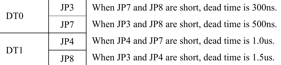
The EG8010 has a fixed switching frequency of 23400 Hz that makes a pulse at 50% duty cycle time duration of roughly 21µs.
That makes the ratio of dead time to pulse length quite important at 1.0 and 1.5 µs, and may impact scaling up for higher output power. The default is 300µs. That is still quite conservative.
Check your MOSFET specifications for minimum dead time requirements.
Soft start
EGS002 has a soft start 3 second feature enabled by default through JP2. I do not recommend disabling this feature.
Voltage feedback & regulation.
It doesn’t look like there are any rectification on the voltage feedback network, nor on the EGS board or outside. and the RC filter made with R4 and C4 has a small time constant of 1ms. The voltage regulation uses a peak detector and measures error in relation to a 3V reference as per datasheet.
In any case the voltage nominal setpoint is performed through the lower leg of the voltage divider using R23 (a 10K potentiometer). A slow acting external voltage control could be done by replacing R23 with a current DAC.
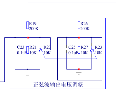
Bipolar switching voltage regulation
You will see in the EG8010 datasheet that the voltage divider network is more complex (it is outside the ASIC board) than for unipolar, with a ganged potentiometer R23. I also suspect missing connection dots in the schematic between R19 and R21 and also R26 and R27 and also at R27 low leg and GND.I will test it on my LTSpice model, so take that info with a grain of salt. Here is the relevant section of the schematic with the proper corrections
Overcurrent protection.
The method employed is a hard current limiter. It cuts the SPWM input to all MOSFET drivers if the output current goes above the setpoint for more than 600ms. The unit is shutdown for 16s, then it will turn on for 100 ms, check for current status and repeat that 100ms on time every 16s if the issue persists for a maximum number of 5 cycles. if the issues persists it powers off and a hard reset is required. If the issue is cleared for more than 1 minute, the state machine resets overcurrent status to nominal.
The board also uses a LM393 OpAmp to process the IFB feedback to shutdown the Gate drivers directly through their SD pins, it is much faster and failsafe than doing this only through the ASIC.
There does not seem to be any soft limiter for light or moderate overcurrent protection (that would lower load voltage for resistive and inductive loads)
A soft limiter would not help for Active loads such as AC/DC PSUs because they change their apparent impedance to compensate for voltage loss.
Monitoring and UI
The monitoring is done through a LCD interface using I2C LCD compatible modules specified in the datasheet to display basic information. Or it can be done through the serial link if you expose the pins properly.
Leave a Reply