EGMicro EGS005 board review
The goal of this post is to analyze in detail the advertised features of the EGS005 board, and show possible modding hacks.
The EGS005 board is the newest board provided by EGMicro for single phase and multiphase inverter designs.
It is based on the EG8025 ASIC that features integrated MOSFET drivers for a full bridge configuration.
Most if not all all of the EGS005 information is also provided in the EG8025 datasheet, plus many more details! We will use the EG8025 datasheet as the reference material, but also compare them to the EGS005 board features, to see what features are restricted by the board.
The EG8025 datasheet is available on the EGMicro website, chip center section.
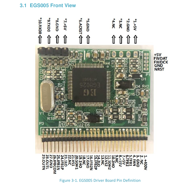
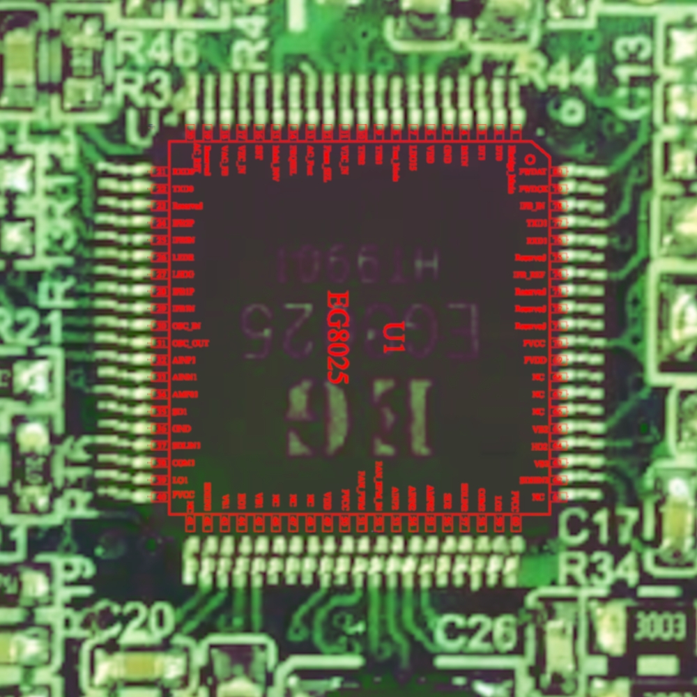
Pinout analysis and IC orientation.
Based on the application schematic and components names and indexes placement, and after boosting trace contrast, it seems pretty evident that this is the ASIC orientation on the EGS005. The D4, D5 diodes and the C17 capacitor with its traces clearly shown going up to the pin, plus the 3 NC pins at the bottom and at the right side make it the only possible configuration. This setup would make the pin1 orientation dot in the product image misleading.
Differences between EGS002 boards and EGS005 boards
We will focus our attention first to the differences in features between these two boards. This takes into account only the features exposed through these two boards, not the overall feature differenciation between EG8010 and EG8025.
EGS005 has these additional features compared to EGS002 :
- integrated MOSFET drivers
- Test mode for SPWM output bench testing without any control loop feedback
- overload protection (not only overcurrent hard limit)
- Two over temperature control zones (IGBT/MOSFET and PCB)
- SPWM signals routing swap on/off between left bridge and right bridge MOSFETs
- AC output enable/disable through pin (basically a soft shutdown)
- Exposed Serial interface (RX and TX), but configuration settings registers besides switching in and out of “Test mode” are either unavailable or undocumented.
- Exposed pins for firmware update
EGS005 features that are discontinued compared to EGS002 :
- Variable frequency output mode up to 100Hz or up to 400Hz. This includes variable frequency mode and fixed ratio V/F mode.
- Choosing between unipolar and bipolar SPWM. Note that EG8025 supports phase synchronisation/phase shift for 3 phase mode, so the modulation scheme had to be made unique for interoperability.
EG8025 features not exposed in EGS005 :
- Phase shift mode for AC sensing from another unit – Phase_SEL pin 12
- AC input for phase synchronization/shift from another unit – VZC_IN pin 17
- AC output for phase synchronization to another unit – AC_Fout pin 13
- Multi inverter pin for parallel operation or master/slave select for three phase operation – Multi_INV pin 15
Inverter phase synchronization and phase shifting
Inverter phase synchronization is required for the following operation modes.
- Parallel mode of operation of two or more inverters sharing a single phase for load sharing / redundancy.
- Parallel mode of operation between one or more inverters and the AC grid, These inverters are known as Grid tie inverters. They are ubiquitous in renewable energy systems for residential or industrial use.
- Parallel mode of operation between inverters or between inverters and AC grid, who do not share the load for redundancy (active/standby system). The phase is kept synchronized between the sources for seamless operation of an ATS (Automatic Transfer Switch). This is to limit potentially high dV/dt (and/or high dI/dt) that happen during switching when the phases are not synchronized.
- Multiphase mode and inverter daisy chaining (cascade) of phase synchronization across usually three units, for three phase power applications, In a (master)/(slave/master)/(slave) configuration. Parentheses correspond to the three inverters.
There are several digital algorithms and analog tehcniques to implement phase synchronization.
One well known and ubiquitous method used in various electronics designs not limited to inverters is PLL (Phase locked loop). There are however other methods. This paper discusses them in detail :
Recent advances in synchronization techniques for grid-tied PV system: A review
https://www.sciencedirect.com/science/article/pii/S2352484721008118
EG8025 Phase synchronization
The EG8025 ASIC uses the Zero Crossing method. It is simple and straightforward.
It uses 2 pins for configuration. Multi_INV pin 15 and Phase_SEL pin 12 and 2 pins for synchronization data. One is an output pin, AC_Fout pin 13 the other is an input pin VZC_In pin 17.
Parallel operation mode
We’ll assume that we use two inverters.
In this mode both inverters share the load on the same phase. One unit is designed as master and has Multi_INV pin 15 pulled log to GND, The other is designed as slave and has Multi_INV pin 15 pulled high to 5V.
The master unit also has VZC_In pin 17 and Phase_Sel pin 12 pulled to GND. Since the master is the start of the synchronization chain, it won’t use an input ZC signal, nor it should shift the phase 120° for parallel operation. Applying phase shift in this mode of operation could destroy both inverters output stages !
The master outputs its phase information through the AC_Fout pin 13. This is a zero-crossing signal. It probably converts upward going zero-crossings of the AC phase to logical HIGH, and downward going zero-crossings of the AC phase to logical LOW. Rising/Falling edges should happen at the time of the zero crossings. Checking precisely the logical levels correspondence is required if this board is to work with another unit of another manufacturer supporting ZC synchronization, to prevent a 180° out of phase condition. Level shifting may be required to accomodate the slave unit.
The slave in turns gets its ZC information on the VZC_In pin 17. The path between AC_Fout pin 13 of the master and VZC_In pin 17 is isolated with the use of an optocoupler. Check figure 10.a of the 8025 ASIC Datasheet. On the slave unit Phase_Sel pin 12 is also pulled to ground while AC_Fout pin 13 is floating.
Since AC_Fout is a low impedance pin current source, it should never get pulled to GND.
Modding for parallel operation.
We should investigate the board and the EGS005 application schematic to look at the trace routing of VZC_In, AC_Fout, and Multi_INV.
Modding fo the slave unit :
- VZC_In is pulled to GND through the R45 1k resistor. Making the VZC_In as an input as shown in figure 10.a would require soldering out the R45 resistor and supplying the signal to the exposed pad of R45 connected to the pin. This signal comes from the optocoupler voltage follower.
- AC_Fout and Phase_Sel do not need any mod on the slave unit.
- Multi_INV trace to GND should be cut and a patch wire soldered and connected to 5V HIGH level
Modding fo the master unit :
- AC_Fout is floating on the EGS005 so a simple wire patch to the pin would do the trick. This wire would be routed to the optocoupler diode anode.
- Multi_INV and Phase_Sel do not need any mod on the master unit.
For a tutorial on how to perform SMD pcb wire hooking look at :
Leave a Reply