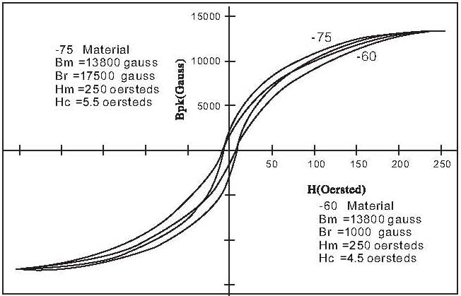
Ltspice Model of an isolated, 48V to 400V, 1600W, Push-Pull converter using Chan model inductors, using the LTC3721 IC.
And detailed design information
Disclaimer:
The following design comes with no guarantees whatsoever. Although a decent amount of time has been spent to ensure that the model works well over the whole range of its design constraints, some errors may still linger, Some more experienced engineers may find some design choices questionable, If you’re able to optimize it or build something better around it, that’s nice.
The choke inductor and the transformer may be a little over-engineered and drive the costs up, given the large ferrite core choices.
You may be able to extract more power than 1600W, but tread carefully.
Additional Resources :
The download is available at the end of this article.
There is also the ‘sister project’ to this one, which performs 230V AC to 48V DC conversion, with the intent of battery charging : It is designed to allow current/voltage control via DAC and a digital potentiometer, so you can digitally control voltage and current and design a charging program.
It is available here :
Abstract:
The main goal of this model is to serve as an aid in learning about the Push pull converter topology,
it also could prove useful when building a prototype, as a part of a UPS or solar converter design.
Care has been taken not to overburden the simulator and allow reasonable simulation speeds.
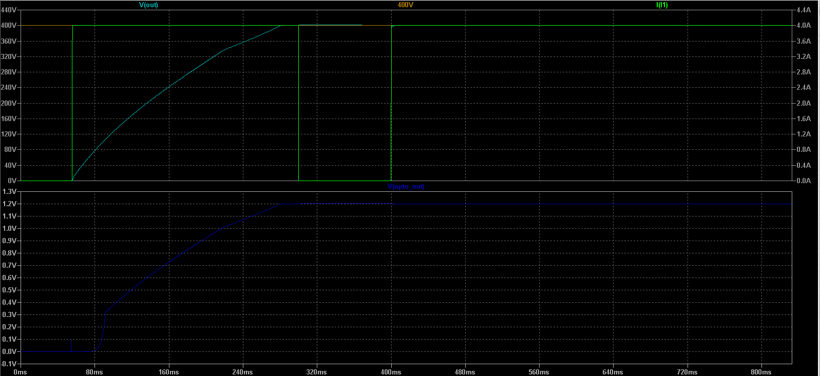
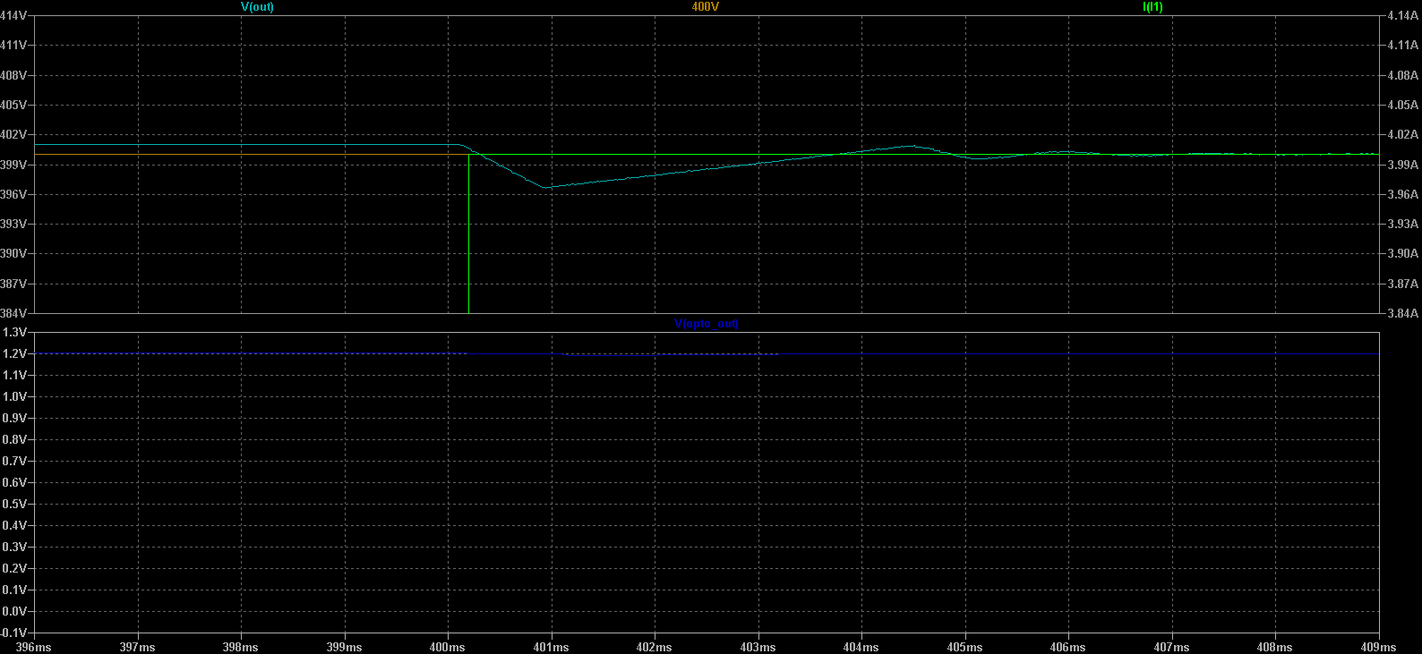
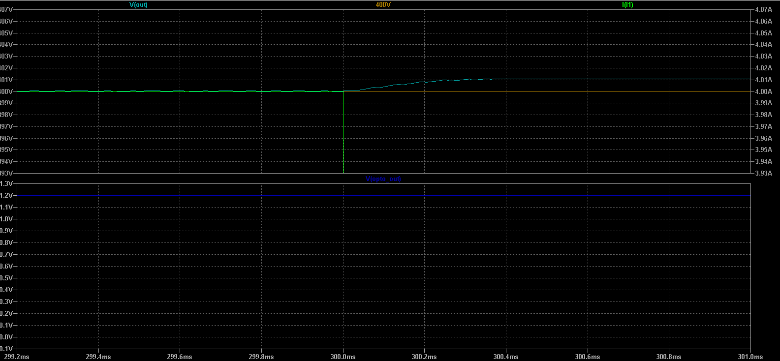
Most of the simulation time is spent ramping up the voltage (soft start)
Using smaller starting loads and stepping them once the converter is fully started decreases simulation time, Once you’ve determined that the soft start ramp is ok.
Intended Audience:
Makers or junior power engineers with little experience, looking for a project that can lead to prototype build.
Three models are supplied :
- The fastest one uses linear inductors, voltage sources for IC power, no isolation, and a simple feedback circuit without optocoupler isolation.
- The second one is the same as the model above but with non-linear inductors (Chan model)
- The full model uses proper and more realistic component DC supply schemes as well as non-linear inductors, as well as isolation. Note that Ltspice is not always able to process isolated secondary circuits, even with the use of a stitching resistor, unless it is very low resistance. Here the problem appeared so we linked both grounds. A practical circuit, of course, will not have that constraint.
Design Parameters
- Max continuous power, 1600W max. Inductor Thermal effects are not modeled, derating may be advisable, Although a large saturation margin has been taken into account.
- Input from 48V (discharged battery, UVLO threshold) up to 57.6 (bulk charging voltage when a charger is connected)
- 400V DC output. it supplies the same voltage as a PFC would.
- This allows easier load switching or load sharing between the battery source and the AC / PFC source converter and can be adapted to larger designs.
- Optimized for high power.
- Moderate to good efficiency 0.93
- Low cost. (uses powder core inductors)
- Fully isolated design.
- Under Voltage lock-out set at 48V to prevent battery bank over-discharge
- 4mm² wire for primary of transformer, 2*24 turns, center tapped
- 1.5m² wire for secondary of transformer 2*234 turns, center tapped
- T400-26 transformer core (Iron powder)
As said before, it is for teaching or training rather than commercial purposes.
It will require hand winding of the toroid to build a prototype. (which is a cumbersome and long process, It is advised to watch several videos about that art to do it properly the first time. (You do not want to rewind it a second time). Building a toroidal transformer is a valuable learning experience.
Some Toroid Winding tips :
Use proper dielectric insulation between windings to control parasitics, it also serves to protect the windings from abrasion.
- Use a counter to keep track of turns.
- Keep the winding tensioned so it does not spring back.
You can also ask toroidal transformer shops to build you a custom transformer according to your specifications.
Proper care has to be taken to balance the primary windings around the center tap as equally as possible to avoid flux imbalance. Fortunately, the number of turns of the primary is low. - Strategically place the tap halfway through the core height, and wind the primary legs as symmetrically as possible, by adequately controlling the winding pitch. Looking at resources explaining the proper way of transformer tapping is advised.
- To make enamel wire solderable, I usually use abrasive dremel cylindrical tips. Do not use a flame as the enamel is very flame resistant and that will anneal the copper making it more fragile.
- You can also watch videos from HAM radio makers, as a lot of them have mastered the art of core winding. A balun is not exactly the same as a push-pull transformer, but a lot of practical building tips apply.
- Always check the final product inductance while testing on exposed wires, with a margin of excess wires so that you can always add turns if inductance falls short. Fortunately, transformer inductance is not that critical, what is critical is balancing and the turn ratio.
Note that It will be hard to find an exact turn ratio from commercial solution catalogs, but you can always look for and adapt the design accordingly. A different ratio will affect the minimum and maximum duty cycles of the converter which could make achieving the 400V target harder at the nominal output load of 4A.
Capacitor Considerations
Input capacitors do not need to be large because of the low battery impedance and stable voltage.
Output capacitors should be low ESR, We choose expensive high capacity, high-voltage electrolytic capacitors to maximize hold time and for lower ripple, and to make the choke
sizing reasonable.
Hold time considerations mostly depend on the load parameters
Additional 450V MPP film capacitors were used. Do not use X2 line capacitors as they are designed to fail short.
MOSFET considerations.
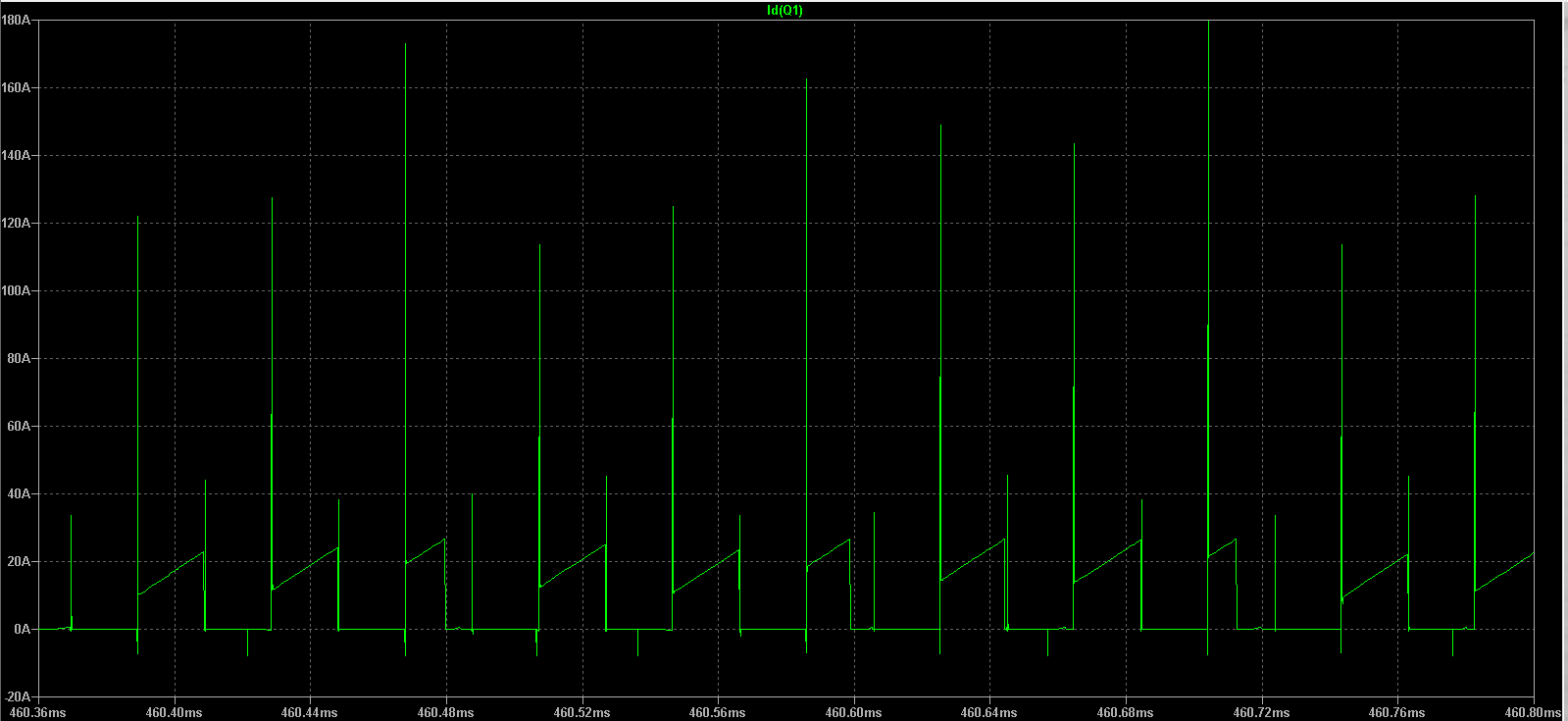
In our design, each MOSFET is subjected to 25 A average current with peaks of up to 120 A due to parasitics (at turn-on), with low-value gate stoppers resistors.
Infineon’s IPP110N20N3 are rated at Id of 88 A and pulses up to 352A.
The datasheet is available at :
https://www.infineon.com/cms/en/product/power/mosfet/n-channel/ipp110n20n3-g/
Thermal management of MOSFET is of utmost importance a clever prototyping solution could make use of radiator/fan bundles designed for CPU cooling, as they often integrate heat pipes, This would complicate the layout significantly and the total prototype volume because of the sheer bulkiness of these kind of components, and require drilling the heatsink backplate. A single modern and standard CPU heatsink fan can cool loads of around 100W. Calculate maximum MOSFET losses and design the solution accordingly.
Never operate MOSFETs under load without proper thermal management!
Overcurrent Protection.
The Switching IC provides a hard current limit that stops switching in case of overcurrent and a resume algorithm explained in the datasheet. For soft current limiting and output CC, you’ll have to implement a current monitor yourself and a feedback signal that overrides the CV signal fed to the optocoupler in case of an overcurrent situation that would decrease output voltage.
Transformer considerations: turn ratio, switching frequency, minimum inductance.
Check this resource for basic formulas.
https://www.analog.com/en/technical-articles/high-frequency-push-pull-dc-dc-converter.html
Also, check :
http://tahmidmc.blogspot.com/2013/03/output-inductance-calculation-for-smps.html
Inductance range tolerance is high since the push-pull converter is based on transformer action. It is not a critical design parameter.
The allowable duty cycle range will dictate the maximum voltage differential between the primary and secondary, in combination with the output voltage range. The fact that the input could already be thought of as regulated (it is a battery, but may be subjected to higher voltages seen by the converter during charging) and that the output voltage is designed to be kept constant eases the design.
It is however important not to drive the core into saturation, So we have made the choice of a large T400-26 iron powder core, although thermal effects (and the decrease of inductance caused by it, will play the limiting role rather than saturation. Here the margin is <add figure>
A larger core also allows a lower fill factor which will improve cooling and reduce ohmic heating from the current flowing into the conductors.
It also makes manual construction easier.
As said before Controlling the winding balance in the primary is critical in Push Pull converters.
An imbalance gives rise to a Bias flux buildup that decreases efficiency.
A low fill factor also allows better cooling performance, even more so if forced (fan) cooling is used to blow axially through the core.
When building a transformer, optimization is complex because of the large parameter domain.
For such a design, it is advised to perform a faster simulation using a standard LTspice coupled inductor,, and specify coupled linear inductors inductance based on Push Pull converter design formulas, and check that the circuit performs ok on that basis. taking care efficiency changes into account with each parameter changes, and performing load stepping, and voltage input range stepping. Efficiency should be high using a fully linear transformer.
If not, something is amiss. Remember that efficiency also depends on load, and is usually lower at very light loads.
On the basis of this first design iteration look at the current flowing through the primary (RMS and peak values), and knowing the number of turns you’ll get the H field strength, which will be used to get the B field strength. B = H/(µo*µr) Then you can look at material tables and check that you are operating within a safe margin. It is a bit complex because there are derating factors, for instance, because of frequency.
Thermal runaway is the situation you want to absolutely avoid (It decreases inductance, which increases the magnetizing current, making the core saturate even more and induces losses which translate into thermal runaway)
Our strategy is low-cost-driven. We choose low permeability iron core and decreased switching frequency to minimize core losses. (iron powder cores perform better at lower switching frequencies)
Iron powder cores are low permeability because of the distributed air gap between magnetic particles, and exhibit high (around 1.5 T) and soft saturation.
For the main transformer, we choose the low-cost 26 Material, and selected a large T400-26 core, allowing higher fill factors. The transformer turn ratio requires a large turn number for the
secondary.
For the output choke, we used a lower permeability 18 Material and a quite large stacked core. Output inductors/chokes operate at a high current bias level so that it derates inductance. Inductance value is also a critical design parameter. When using a suboptimal (too low inductance, output ripple, and inductor heating will be higher, with also a risk of thermal runaway and gradually decreasing stability.) We noted that when using too low inductances, the design refused to reach our target voltage, Which seems to be a protection feature of the converter IC.
To sum up, We have to obtain an inductance large enough for our filtering goals at nominal power while
reducing the bias B field. B field is proportional to the number of turns times permeability, all other parameters being equal, while inductance increases with the square of the number of turns times permeability. Thus it follows to use a larger core with lower permeability to accommodate a larger number of turns to meet inductance requirements while staying under saturation levels. To lower the B field, we also used the stacking strategy to increase the total compound core area. It is easier to wind that way than individually winding inductors and placing them in series, on the board, especially if PCB real estate is a concern. It would however decrease cooling efficiency. Not seen much about that method in commercial products, as it could also increase flux leakage. Better test it.
EMI concerns.
The low-frequency operation of 25Khz reduces EMI concerns depending on regulations on that VLF band and the other components that may be subjected to it. It is above the audio hearing range, but some harmonics may find their way into audio equipment (The IC switching frequency may go up to 1Mhz, changing the frequency would require choosing a better-suited, ferrite instead of iron powder material and adapting core dimensions, usually smaller ones. However, we had trouble making the simulation run smoothly at higher switching frequencies. Higher switching frequency also has a dramatic impact on simulation performance, as the minimum timestep has to be lower.
Of course, general layout guidelines apply, such as reducing the loop area of switching components traces paths (MOSFET drain to source) and the length of gate signals. Shielding is an option if it does not interfere with cooling.
Lower frequency however could make the core produce an audible stridulation effect, because of the magnetostrictive effect that is close to the audible range.
Core design helpers :
Our advice is to use a Ltspice core test bench using the resources here :
https://www.eevblog.com/forum/projects/arbitrary-%28saturable%29-coupled-inductors-in-ltspice/
For more information about the Chan model :
https://ltwiki.org/index.php?title=The_Chan_model
You will also need these very useful resources :
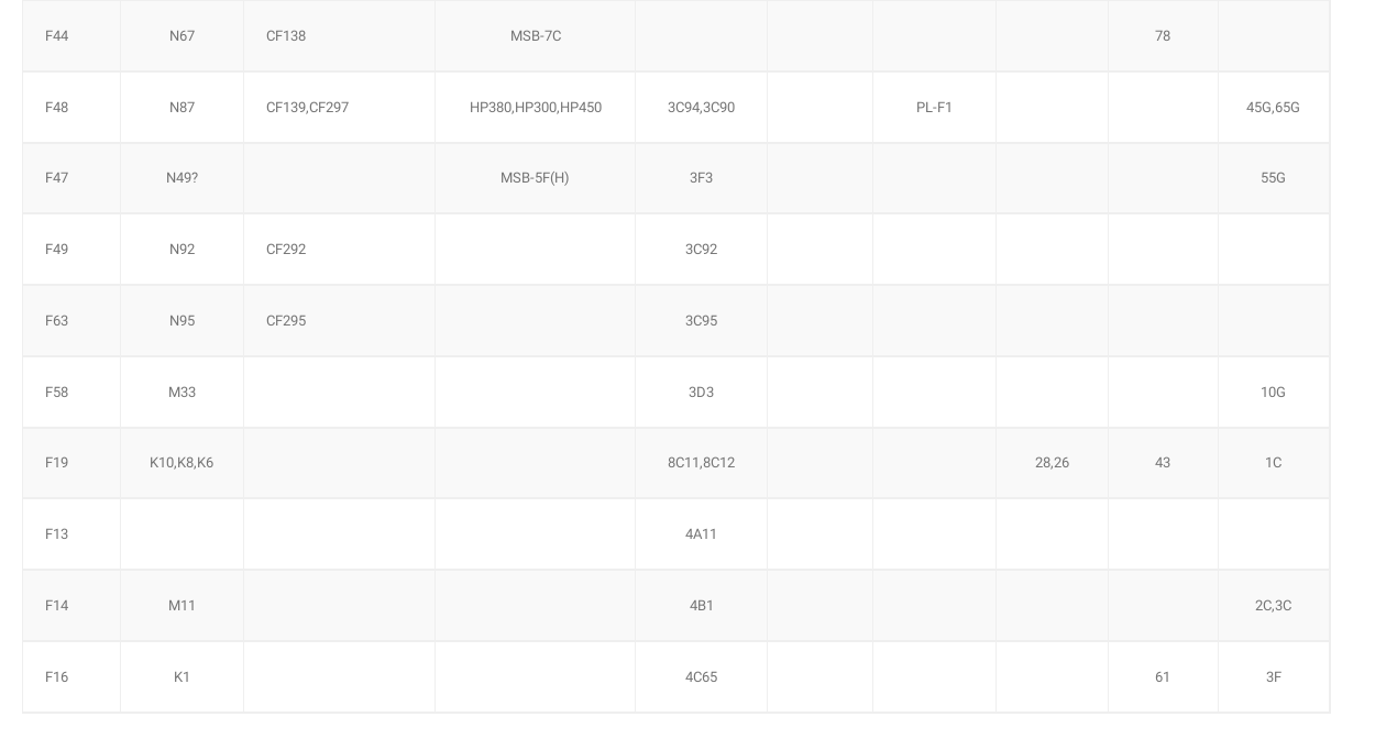
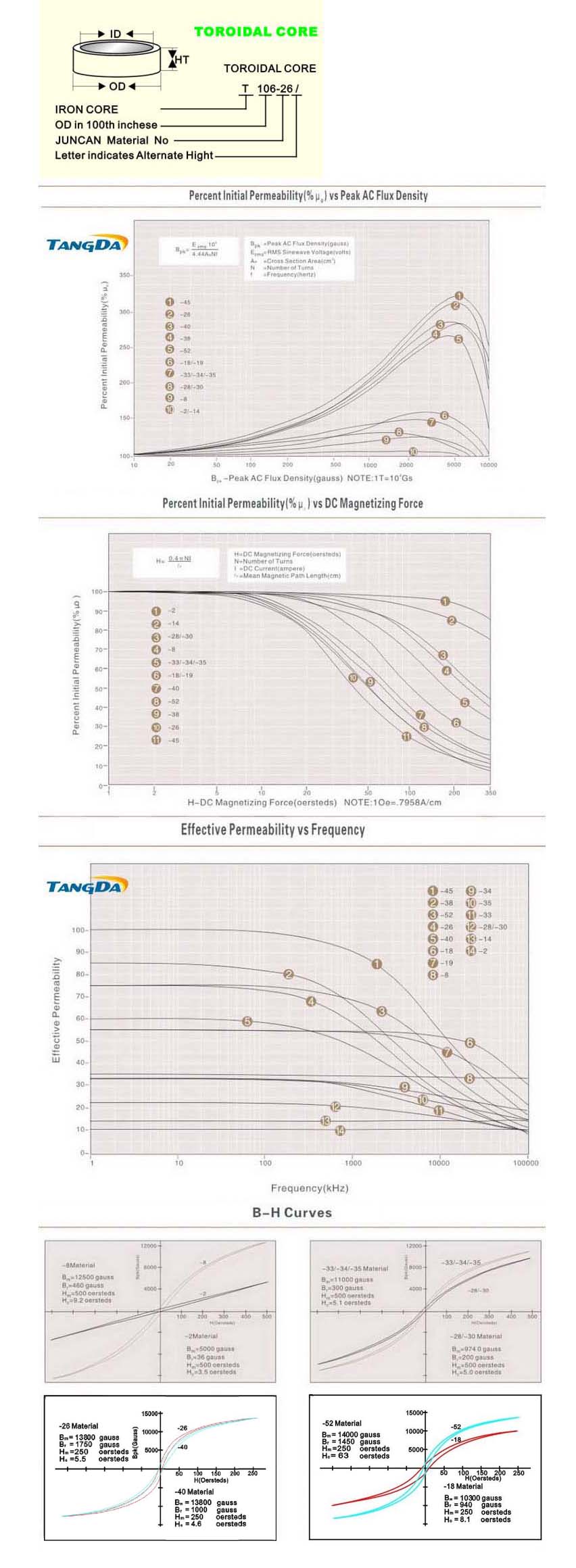
- Magnetics catalogs and materials datasheets from major Western manufacturers: TDK Epcos, Ferroxcube, Magnetics.inc Micrometals,
- The same for Asian ones: JUNCAN, Tangda, Caracol, etc… A popular seller is Tangda if you need to source (relatively) cheap cores from China.
- The B/H curves when you can find them, if the Chan model parameters are not specified.
- Magnetics cross-reference lists, images and pdfs. This will make selecting cores a littles easier, when switching from one manufacturer to another.
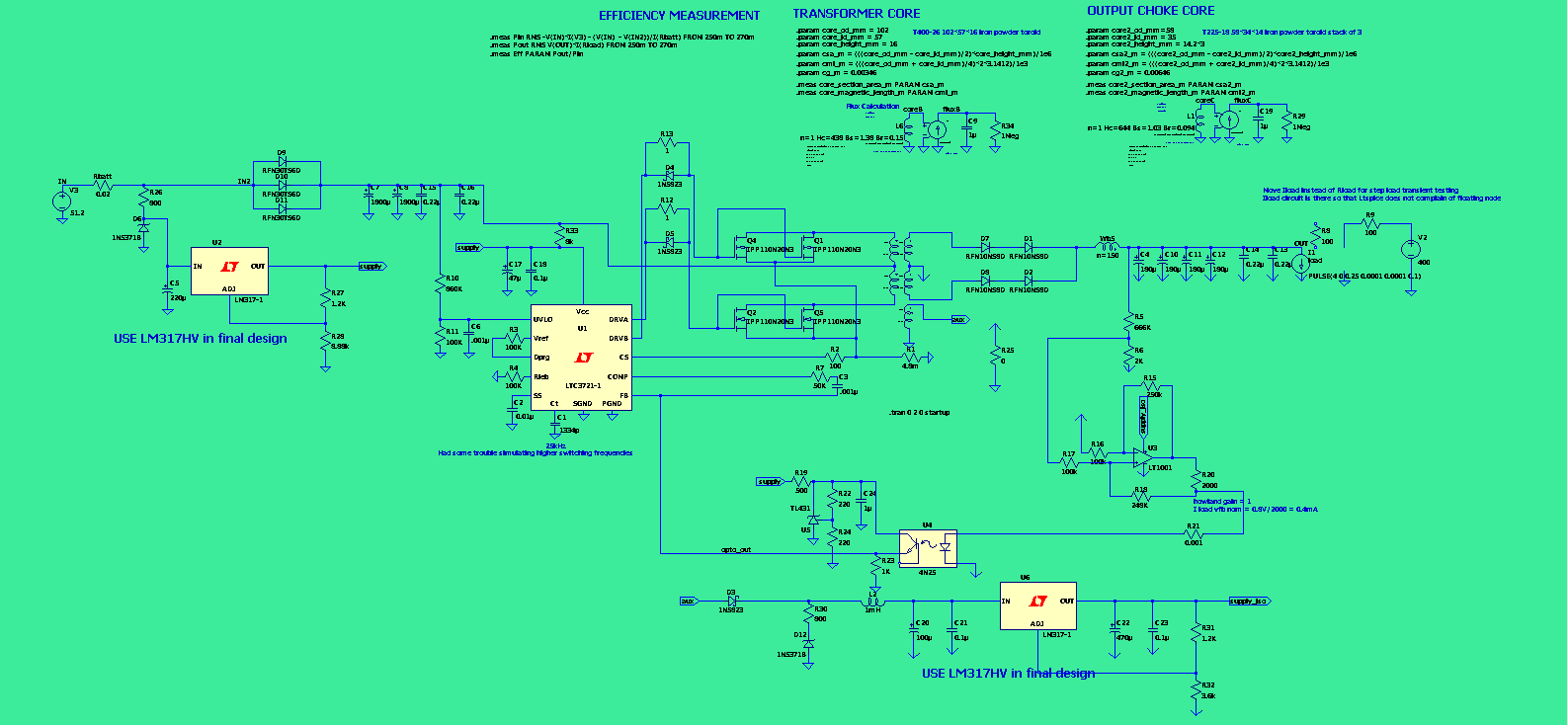
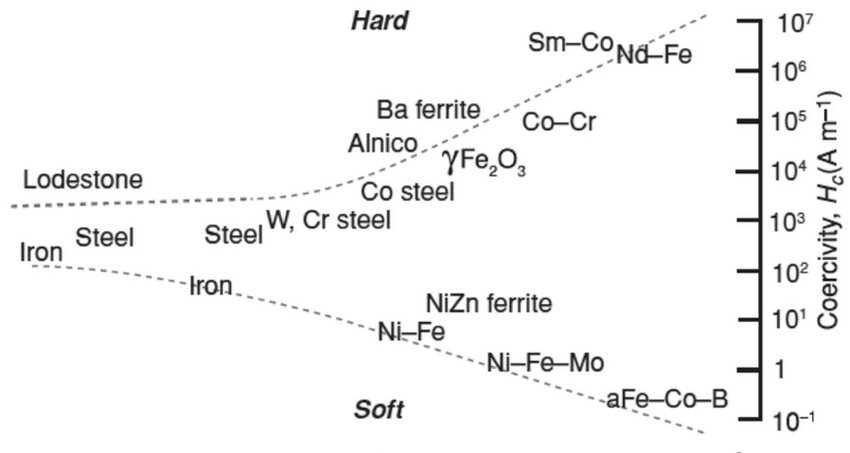
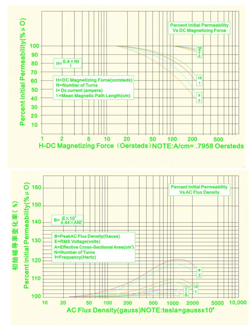
If you need to look at a B/H curve or if you have experimental data from a B/H curve tester (usually pluggable to an oscilloscope), you will need to find the crossing points on :
the B axis (y) : for Br (B field – remnant) and Bs (B field – saturation)
and the H axis (x): for Hc (H field – coercivity).
Bs is the saturation (horizontal asymptote line B value) for hard saturation, for soft saturation it is determined differently, as the B field keeps increasing, albeit with a lower and lower slope.
A good rule of thumb for soft materials is to stay in the linear region, with a good (30 to 40% margin)
Fortunately, Chinese manufacturers provide the B/H curves and Br, Bs, and Hc.
With all these collected data, you are ready to test the cores in the Ltspice Chan model test Bench.
- Use the manufacturer-supplied geometric data OD, ID, and Height. We updated the test bench with geometric data calculators for the magnetic length and area required by the model.
- Input magnetic data for the Chan model, taking care to use SI units: Hc (A/M), Br (T), Bs (T), (Amperes/m and Tesla)
Alas, Western Manufacturers usually provide the Al value and Bs (B sat) but almost never an exploitable full BH curve. You will need to contact them for this, but it may be a trade secret, who knows?
What you can do however is parse scientific publications to get harder to find values such as Hc and Br, and the problem is that they come for generic alloys (says MnZn, or very exotic ones) A comprehensive database of core parameters is clearly needed at this point.
If the data is in Oersted and Gauss, multiply the Oersted value by 79 to get A/m and for Gauss divide by 10000 to get Tesla units.
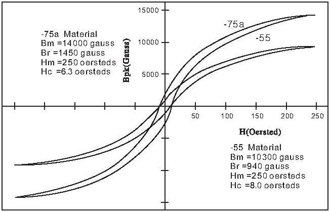
Some reference data, mostly for iron core materials collected that you may find useful :
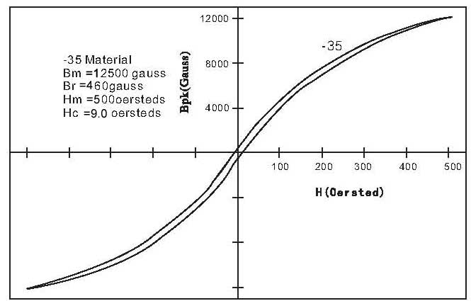
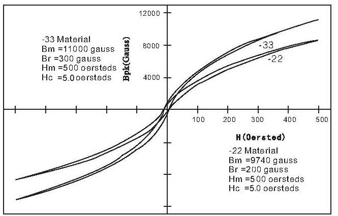
An important note that I have not confirmed at this point: Note that the Iron powder materials data found on Chinese resellers are (presumably) for a pure (no distributed gap) material, thus if you plug the data into the mag_inc_bias.asc, you’ll find an abnormally large Al value.
So the strategy is to set primary_turn in the test bench model at 1, and play around with the core Chan model parameter Lg (gap length value in meter), until you obtain the nH/t^2 that is specific to the core.
Remember to set I_bias to 0. There is also a 60nH inductor in series, that would need to be set to 0 for adequate measurements of very small inductances.. I have no idea what is the purpose of this.
SUMMARY OF INDUCTOR TEST BENCH SETUP
- Create one asc file based on mag_inc_bias for each core (makes life easier)
- Fill in geometric data
- Fill in material data (Hc, Br, Bs)
- Set primary_turn to 1.
- Set I_bias to 0.
- Find distributed air gap equivalent gap length L_g by trial and error (examine inductance .meas in the error log) until the inductance value is equal to datasheet Al.
This is particularly useful to test for inductance decrease due to I bias current (seen in the output inductor choke)
If you need to lower the testing frequency, you’ll need to increase the simulation time because the measurements use 15th/16th cycles of RISE/FALL for inductance measurements, otherwise, you’ll get “measurement failed”
Inductance measurements are required for the choke, for the transformer, just check that the B field remains under Bsat with some margin.
Note that the I1 source is used for inductance measurements (It is set at 1mA, thus the x1000 factor in inductance measurement)
The measurement is based on the formula V = Ldi/dt, L = V(dt/di) = V/freq2pi at zero cross.
Increasing I2 will decrease inductance This is used for the choke measurement (under DC bias). Test with I2 value equal to the max allowable output current, with the frequency set correctly and the choke turn number set correctly.
Verify that the inductance value is still above requirements and that the B field in Tesla is not above Bsat.
As a final note, It should be said that the Chan model has been superseded by the Jiles-Atherton model which shows better fidelity to the experimental BH curves.
Unfortunately, Ltspice models using the JA model (CoreJA) are prohibitively slow for use in power product simulations, But the test bench could be adapted using CoreJA. The advantage of the Jiles Atherton model is that you can find a database of JA parameters for a lot of cores in the magnetic.txt file of the ZZZ library. This is the famous Bordodynov library (also known as the Yahoo Ltspice group library or the Ltspice groups.io library) It is a must for every serious Ltspice user.
Software also exist that help in complete solution design with an emphasis on magnetics, such as ‘ExcellentIT’, and also good product finders on manufacturer’s websites, to help in core selection.
Once you have made a provisional choice for the cores, turn number and turn ratio, you can replace the linear models using inductances with the Chan model using the turn number.
The Chan model slows the simulation speed only very moderately.
Isolation
This is an isolated design, However, Ltspice complains when using separate grounds, unless stitched by very low resistors. here we used a 0 ohm resistor between GND (primary ground)
and COM (secondary ground) in practice of course there is galvanic isolation.
Optocoupler tuning
We used a TL431 to provide a stable 5V reference required by the optocoupler output transistor.
To provide current to the optocoupler diode we use a modified (improved) Howland current pump.
Using a simple shunt resistor of around 240k to control the current flowing into the diode induces noise in the simulation. It should be tested in practice. The advantage is that such a solution would be passive and not require a low-voltage DC supply operating on the isolated side.
More information about the improved Howland current pump is available here :
https://www.ti.com/lit/an/sboa437a/sboa437a.pdf
Compensation network
Compensation network time domain testing :
Replace the passive resistor load with an active load (flagged as load)
The compensation network can be tested for stability by stepping the active load, and examination of the induced voltage oscillatory response, its amplitude, and its damping characteristics.
For more information on compensation networks :
https://www.analog.com/media/en/analog-dialogue/volume-57/number-2/step-by-step-process-to-calculate-a-dc-to-dc-compensation-network.pdf
Ltspice (the latest version) also offers transient frequency response analysis. It combines transient analysis (so that the circuit operates normally), while a small signal
stimulus is provided on the input voltage side. The small signal response on the output is analyzed so that a Bode Plot can be drawn and analyzed for stability. (checking gain margin and phase margin taking into account the switching frequency vs the frequency location of poles and zeros.)
Combining frequency analysis with a transient analysis has the advantage of not requiring specialized frequency response models for IC (When they are available)
In this model, the input voltage is stable, Output capacitance is large with a low ESR, which helps for stability. A good test would be to introduce a disturbance by simulating a charging operation in the bulk (constant current) charging phase.
Powering up the IC, the Optocoupler, and the current source OpAmp
The switching IC has access to the primary side power battery power. As it is a well-behaved supply, no need to power the IC from an auxiliary winding from the main transformer. Powering the IC is documented well on the IC datasheet. In our case, however, the design is simpler.
Note however the presence of the R33 resistors that shunts some current from the primary DC link into the IC, charging the capacitor faster, than what the LM317 alone would do, and allowing the IC to start faster, The datasheet uses a 2k value for ar 12V primary, we just scaled it linearly.
In this design, we used a simple LM317 regulator, which may be used to power other logic loads. The LM317HV version tolerates the battery bank voltage. You can also use a lower voltage version and power it from a single battery unit closest to ground, Which would have its positive terminal sitting at 12V above primary ground. Note that the IC is internally regulated at 10.5V or so, and can operate as per datasheet with as little as 8V. We found that it needs 10.5V during startup, and we set up the LM317 to supply a constant 10.5V. The absolute maximum rating is 12V. We also used a pre-regulator high voltage 60V Zener to protect the LM317 in case of a voltage transient. (Which could come from the charging operations)
For the secondary, things are a bit more complicated. The only active component here is the OpAmp of the Howland current pump driving the LED of the optocoupler.
In reality, it is almost guaranteed that other logic or control components will be operated at low voltage with a secondary ground reference. Thus we used a 5V setting for the secondary side LM317, This low voltage did not seem to affect negatively the operation of the Howland current pump opamp
We could assume that the 400V link always has access to power, for instance, a rectified mains AC power source output from a 400V PFC unit.
In UPS and solar applications, that may not be always the case, take as an example the “cold start” of an UPS from the battery in the absence of mains power.
The absence of power to this component means no voltage feedback signal to the switching IC. It needs to power up quite fast (well before the secondary reaches 400V DC)
For this, we use a secondary auxiliary winding, a rectifying diode, and an LM317 set up for 5V output to power the OpAmp. The LT1001 Op-amp. is fully turned on at around 2.5V
An optional Zener could be added as a TVS function to clip transients above the LM317 rating.
MOSFET parasitics, ringing, and leading-edge current spikes.
Figure 4 shows leading edge current spikes, they are not associated with ringing (as they are fully damped). The following thread identifies the culprit as being the reverse recovery time of the secondary side rectifying diode as well as the gate pulse. To minimize these effects, One can use fast recovery diodes for the secondary rectifier, as well as to increase the gate stopper resistor values (but the latter has drawbacks, as we’ll see in a moment). Reducing these spikes by using fast recovery diodes may increase overall efficiency, as well as decrease HF EMI (the spike frequency is substantially higher than the switching frequency).
In our simulation, the current spikes are well under the 352A max pulse current specification of the MOSFET, so it should not damage the MOSFET over the long term. (When using standard silicon diodes for the secondary’s rectifying diodes.
Voltage transients and ringing.
Although this model does not exhibit this unwanted phenomenon, it is probable that a real-life implementation would because of parasitics that are not modeled here.
Ringing comes from MOSFET parasitic capacitance, coupled with the driven circuit (a transformer) inductance as well as trace inductance. Most of the push-pull converter designs come with some sort of snubber (RC series circuit across drain and source, tuned to the problematic ringing frequency), However, Value tuning is quite layout dependent. Having broad but short gate traces also helps in the management of the problem. make sure your layout accommodates some room to add a snubber.
A resistor gate stopper (here 1 ohm) also may help, but its value cannot be pushed too high: You also have to take into account gate capacitance. A large gate capacitance cannot suffer from a too-large gate stopper resistor, or the MOSFET will turn on slowly, and the slow turn-on will increase average Rds. On the other hand, a too-low gate stopper could push the gate currents above the IC specifications, especially if the MOSFET gate capacitance is high. (Which is somewhat the case for high-power MOSFETs) Thus a snubber seems like a good option.
Remember that this part may exhibit different behavior in real life due to the non-modeling of all parasitic effects and their layout dependence.
Using a 4-ohm resistor instead of 1 ohm decreases the peak pulse current from 210 A to around 160 A.
Figures
Model Information
LM317 model as well LTC3721 should be present in a recent Ltspice installation.
You may need Infineon’s IPP110N20N3 model.
This model has been tested on a Ltspice installation using the ZZZ (Ltspice groups.io community library), it is advised you install it.
Leave a Reply