Category Power Electronics Reviews

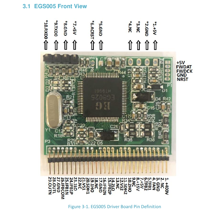
SC-120W 12V PSU with UPS function review.

or How to battery backup your router the proper way.

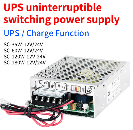
This unit is a good choice to provide long UPS time in an event of a power outage for small but critical loads like an Internet router, Where a full 110V/220V UPS is overkill. A typical internet router power rating is around 15W. Assuming the SC120W is wired to a 60Ah 12V battery and assuming 50% discharge, the router could keep working for almost 20 hours in an outage event.

Voltage Setup.

There is a white screw near the battery cable. This regulates two outputs:

  • The set float voltage of the battery (for a lead acid battery, this should be always set up at at least 12.9V +/- some voltage according to the ambient temperature, but it will be always more in a realistic scenario, the float voltage is between 13.1V and 13.8V. That means that this unit is not made for frequent outage cycles, since it would also cycle charge the battery, and charging is usually done at higher voltages.
  • This screw also regulates the working voltage of the load, minus a diode drop it seems (that is, the load voltage will be the battery float voltage minus 0.6V)

So, for example if you set the battery float at 13.8V, the load will be supplied 13.2V. Routers have voltage regulators inside. As a rule of thumb, electronics tolerate +/- 10% deviation of the nominal supply voltage which is 12V for most routers, Putting 13.2V into the router could damage its regulator over the long term, leading to reduced lifespan.

The proper way to do it : Insert a DC/DC step down module like these based on the LM2596A between the SC120W and the router,

DC/DC Step Down to convert 13.8V into 12.V. The 3A rating is adequate for most routers

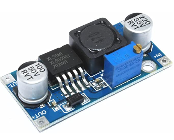
and adjust the step down module to output 12V, now you can set up an appropriate float voltage for the battery without damaging the router.

Charge current limiting.

There are no regulating screws for charge current limiting, so, if you set the voltage too high and the battery is discharged, it could draw current up to the overcurrent protection limit. I did not push the test unit far enough to see if it is 10A or less at (the PSU nominal power rating), Nevertheless, it is recommended to charge a battery at a current no more than 0.1 * total capacity. If you use a small battery, and there are some outages, reduce the float voltage accordingly. Best is to use a large battery so you can setup a higher float voltage, its lifetime won’t be affected by the charging currents which would fall mostly under 0.1 * total capacity, and it will benefit from higher float voltages.

Optional setup for frequent and long outages.

In case of frequent and/or long outages It could be theoretically possible to use a dedicated battery charger to charge the battery using a bulk charing constant current phase, a topping charge, and a trickle charge phase commonly used in “intelligent” chargers, in addition to the SC-120W. This would be done by connecting the battery terminals to such a charger, and a diode between the SC-120W and the battery, to prevent the SC-120W from backfeeding the battery, that is, current flow would be restricted from going from the SC-120W to the battery, only allowed from the battery to the SC-120W. Charging would be performed only by the added dedicated charger. Such a charger should be a model that allows for continuous use.

Overall, it would serve to protect the SC-120W from having to deliver large currents to charge the battery up to its nominal capacity after a long outage where the battery is deeply discharged.

The downside of that setup would be the additional voltage drop from the diode between the SC-120W and battery while operating on battery, as it could bring the voltage into levels below 12V

Ideally, the voltage setting of the SC-120W would have to be setup so that it is more or less the same of what the charger voltage is at its max value minus the voltage drop of the diode, and that is program-phase dependent, To complicate issues more, the voltage drop of the diode also depends on current. Some chargers output high voltages for short periods of time in the equlization phase. Best is to have a good charger datasheet that explains well how the charging is done and allows for a good amount of configuration. Having voltages more or less equal could help in the regulation of the SC-120W. As the circuit of the SC-120W is not published, it is hard to say what would be the behaviour of the unit if it is setup at, let’s say 13.2V and a charger outputs 14.4 V, the SC-120W would then see 13.8V (accounting for the voltage drop of the diode added between the battery and the SC-120W), while its setpoint is at 13.2V

I encourage you to perform extensive and careful testing if you wish to go this way.

Behaviour while in UPS mode.

Voltage regulation behaviour testing should also be performed when the unit is on battery (without AC). Unfortunately, I lapsed to note data from this part in my testing protocol. If I remember well, the voltage seen by the load is then the battery voltage minus a diode drop. That is, the SC-120W does not perform dc step-up conversion to keep the voltage at the setpoint of nominal operation (on AC) Again, this should be tested, as designs may change over time. I will update this material when able to perform the test.

Behaviour on battery power loss / cold start mode

One peculiarity of the unit : If the battery connection is lost during a power outage, and is subsequently regained while the outage remains, or if the unit is connected to a battery to supply a load while it has no AC power, the load will not come online again by itself. There is a little button near the voltage potentiometer that will force supply power to the load, this function is known as a form of cold start.

It may also be possible that this function activates if the battery voltage falls under a certain level, to protect the battery. but I have not tested it.

LED indicator strip

There are three LEDS, on a strip connected to the unit through a ribbon cable. This is practical for industrial front panel installation.

  • One shows that AC is available (red LED)
  • One shows that DC power is supplied to the load (green LED)
  • One shows that current is flowing between the SC-120W and the battery. (red LED) It glows brighter under high current conditions. I suspect this is the “battery is charging” indicator. When charging current settles down, the red LED light slowly turns off. I have not tested if this LED also glows when high current is drawn from the battery.

A final warning.

The battery cable of the SC120W does not have inbuilt fuses. It is always required to implement fuses on battery links. Add a section of cable with male spade connectors (the SC120W battery terminations use female spade connectors) with a fuse in it.

Overall rating.

The unit is sturdy and the UPS function performs very well, (for over a year) and it charges/discharges the battery as advertised. There is 0 downtime during switching events. The only down sides is that is a CV control mode only (no constant current charging phase) and that the system load voltage is related to the float voltage of the battery, Given the price of the unit that’s overall worth it.

There is also a 180W unit. This could also proove a good choice to provide battery backup to larger DC loads like NAS appliances, Beware, some units require a dual +5V + 12V psu, replacing that PSU by the SC180W would require two instead of one, higher rating DC/DC step down converters.

EGMicro EGS005 board review

The goal of this post is to analyze in detail the advertised features of the EGS005 board, and show possible modding hacks.

The EGS005 board is the newest board provided by EGMicro for single phase and multiphase inverter designs.

It is based on the EG8025 ASIC that features integrated MOSFET drivers for a full bridge configuration.

Most if not all all of the EGS005 information is also provided in the EG8025 datasheet, plus many more details! We will use the EG8025 datasheet as the reference material, but also compare them to the EGS005 board features, to see what features are restricted by the board.

The EG8025 datasheet is available on the EGMicro website, chip center section.

Probable IC orientation

Pinout analysis and IC orientation.

Based on the application schematic and components names and indexes placement, and after boosting trace contrast, it seems pretty evident that this is the ASIC orientation on the EGS005. The D4, D5 diodes and the C17 capacitor with its traces clearly shown going up to the pin, plus the 3 NC pins at the bottom and at the right side make it the only possible configuration. This setup would make the pin1 orientation dot in the product image misleading.

Differences between EGS002 boards and EGS005 boards

We will focus our attention first to the differences in features between these two boards. This takes into account only the features exposed through these two boards, not the overall feature differenciation between EG8010 and EG8025.

EGS005 has these additional features compared to EGS002 :

  • integrated MOSFET drivers
  • Test mode for SPWM output bench testing without any control loop feedback
  • overload protection (not only overcurrent hard limit)
  • Two over temperature control zones (IGBT/MOSFET and PCB)
  • SPWM signals routing swap on/off between left bridge and right bridge MOSFETs
  • AC output enable/disable through pin (basically a soft shutdown)
  • Exposed Serial interface (RX and TX), but configuration settings registers besides switching in and out of “Test mode” are either unavailable or undocumented.
  • Exposed pins for firmware update

EGS005 features that are discontinued compared to EGS002 :

  • Variable frequency output mode up to 100Hz or up to 400Hz. This includes variable frequency mode and fixed ratio V/F mode.
  • Choosing between unipolar and bipolar SPWM. Note that EG8025 supports phase synchronisation/phase shift for 3 phase mode, so the modulation scheme had to be made unique for interoperability.

EG8025 features not exposed in EGS005 :

  • Phase shift mode for AC sensing from another unit – Phase_SEL pin 12
  • AC input for phase synchronization/shift from another unit – VZC_IN pin 17
  • AC output for phase synchronization to another unit – AC_Fout pin 13
  • Multi inverter pin for parallel operation or master/slave select for three phase operation – Multi_INV pin 15

Inverter phase synchronization and phase shifting

Inverter phase synchronization is required for the following operation modes.

  • Parallel mode of operation of two or more inverters sharing a single phase for load sharing / redundancy.
  • Parallel mode of operation between one or more inverters and the AC grid, These inverters are known as Grid tie inverters. They are ubiquitous in renewable energy systems for residential or industrial use.
  • Parallel mode of operation between inverters or between inverters and AC grid, who do not share the load for redundancy (active/standby system). The phase is kept synchronized between the sources for seamless operation of an ATS (Automatic Transfer Switch). This is to limit potentially high dV/dt (and/or high dI/dt) that happen during switching when the phases are not synchronized.
  • Multiphase mode and inverter daisy chaining (cascade) of phase synchronization across usually three units, for three phase power applications, In a (master)/(slave/master)/(slave) configuration. Parentheses correspond to the three inverters.

There are several digital algorithms and analog tehcniques to implement phase synchronization.

One well known and ubiquitous method used in various electronics designs not limited to inverters is PLL (Phase locked loop). There are however other methods. This paper discusses them in detail :

Recent advances in synchronization techniques for grid-tied PV system: A review

https://www.sciencedirect.com/science/article/pii/S2352484721008118

EG8025 Phase synchronization

The EG8025 ASIC uses the Zero Crossing method. It is simple and straightforward.

It uses 2 pins for configuration. Multi_INV pin 15 and Phase_SEL pin 12 and 2 pins for synchronization data. One is an output pin, AC_Fout pin 13 the other is an input pin VZC_In pin 17.

Parallel operation mode

We’ll assume that we use two inverters.

In this mode both inverters share the load on the same phase. One unit is designed as master and has Multi_INV pin 15 pulled log to GND, The other is designed as slave and has Multi_INV pin 15 pulled high to 5V.

The master unit also has VZC_In pin 17 and Phase_Sel pin 12 pulled to GND. Since the master is the start of the synchronization chain, it won’t use an input ZC signal, nor it should shift the phase 120° for parallel operation. Applying phase shift in this mode of operation could destroy both inverters output stages !

The master outputs its phase information through the AC_Fout pin 13. This is a zero-crossing signal. It probably converts upward going zero-crossings of the AC phase to logical HIGH, and downward going zero-crossings of the AC phase to logical LOW. Rising/Falling edges should happen at the time of the zero crossings. Checking precisely the logical levels correspondence is required if this board is to work with another unit of another manufacturer supporting ZC synchronization, to prevent a 180° out of phase condition. Level shifting may be required to accomodate the slave unit.

The slave in turns gets its ZC information on the VZC_In pin 17. The path between AC_Fout pin 13 of the master and VZC_In pin 17 is isolated with the use of an optocoupler. Check figure 10.a of the 8025 ASIC Datasheet. On the slave unit Phase_Sel pin 12 is also pulled to ground while AC_Fout pin 13 is floating.

Since AC_Fout is a low impedance pin current source, it should never get pulled to GND.

Modding for parallel operation.

We should investigate the board and the EGS005 application schematic to look at the trace routing of VZC_In, AC_Fout, and Multi_INV.

Modding fo the slave unit :

  • VZC_In is pulled to GND through the R45 1k resistor. Making the VZC_In as an input as shown in figure 10.a would require soldering out the R45 resistor and supplying the signal to the exposed pad of R45 connected to the pin. This signal comes from the optocoupler voltage follower.
  • AC_Fout and Phase_Sel do not need any mod on the slave unit.
  • Multi_INV trace to GND should be cut and a patch wire soldered and connected to 5V HIGH level

Modding fo the master unit :

  • AC_Fout is floating on the EGS005 so a simple wire patch to the pin would do the trick. This wire would be routed to the optocoupler diode anode.
  • Multi_INV and Phase_Sel do not need any mod on the master unit.

For a tutorial on how to perform SMD pcb wire hooking look at :

EGMicro EGS002 board review

The goal of this post is to analyze in detail the advertised features of the EGS002 board, and show possible modding hacks.

The EGS002 board is the oldest provided by the EGMicro supplier still distributed on common Chinese reseller platforms. It superseded the even older EGS001.

It is based on the EG8010 ASIC and also features either two IR2110S half bridge drivers, or two EG2113, an EGMicro driver. Whether you get one or the other depends on the reseller. Check for comments and reviews on marketplace product page to see who’s getting what.

Most if not all all of the EGS002 information is also provided in the EG8010 datasheet, plus many more details! We will use the EG8010 datasheet as the reference material, but also compare them to the EGS002 board features, to see what features are restricted by the board.

EG8010 ASIC Features

Input DC Voltage. The EGS002 can drive high voltage MOSFETs easily. no restrictive voltage limitations on the high side MOSFETs, and it is at least ok for 400V DC input to the MOSFET bridge. Supplied design schematics show power coming through a 400V DC link PFC output.

Inverter output frequency. EG8010 can be used for fixed 50Hz,60Hz or frequency adjustable 0~100Hz or 0~400Hz output.

The EGS002 on the other hand restricts this feature to fixed frequency operation : either 50Hz or 60Hz, through jumpers.

These jumpers are exposed on the bottom plane of the board and are set with solder bridges over two pads. They do not appear to be through hole, so it would be difficult to insert header pins and use a real jumper there.

the backside exposes the configuration jumpers. top left of image

JP1 and JP5 on the board control FREQSEL0 pin 18 level (either HIGH=JP1 short for 60Hz or LOW=JP5 short for 50Hz). They can’t be short or open at the same time !!

Is the board moddable for further frequency control ? let’s see.

There seems to be two methods to apply mods. Either through hardware or through software (by serial commands). Let’s explore the hardware method first.

Variable Frequency mode modification

Up to 100Hz or up to 400Hz variable frequency operation mode selection is controlled by FREQSEL1. It seems however that the EGS002 has the FREQSEL1 pin 19 grounded in the EGS002 schematic. So it depends on the suppliers of EGS002 to create derivative boards that expose FREQSEL1.

As far as I searched on Chinese marketplaces that doesn’t seem to be the case.

PIN 19 and PIN 20 Traces Merge. right around the center of R33. Processed image to better expose the traces

FREQSEL1 pin 19 and MODSEL pin 20. seem both connected to ground in most boards available on the market through merging traces. This is in conformity with the EGS002 datasheet.

That restricts the unmodded board to 50/60 Hz Operation and Unipolar switching

Modding for tests to enable VVVF to 100 Hz or to 400 Hz would require cutting the FREQSEL1 pin trace and patching the pin with maybe AWG30 hookup wires and connect it to HIGH level. MODSEL would be still kept to GND.

JP1 and JP5 would allow to control max frequency to 100Hz or 400Hz.

Note that variable frequency with constant voltage mode and variable frequency with variable voltage both require Unipolar switching. That is why you don’t have to bother with MODSEL in this mod

Once FREQSEL1 is set to HIGH, Variable frequency mode type is enabled through VVVF pin 32. In EGS002 again, it is connected to ground. This mode would give EGS002 the variable frequency constant voltage mode by default. (without further mods)

To enable VVVF variable freq/variable voltage (albeit with constant V/F ratio) for single phase VFD applications, bring VVVF to HIGH

Pin 32 VVVF. For variable frequency mode in unipolar switching

Again, the trace after the pin may be cut if other pins do not depend on the cut trace, which may be difficult to check since some trace may hide under the IC.

Note that there are several test points / open vias on the board that can be used to patch the board with additional connections.

Then you have to expose FRQADJ/VFB2 pin to set the desired frequency in variable frequency mode through an external potentiometer in figure 8.6a of the datasheet. Voltage regulation is still performed through R23 and VFB1

In constant voltage/frequency ratio mode, you use R23 to set the nominal voltage at 50Hz through VFB1 Frequency ratio control goes through FRQADJ/VFB2 in this mode. It is a bit unclear in the datasheet.

Bipolar SPWM enable modification

Remember that you cannot use VVVF features in this mode.

The mod would require :

  • cutting MODSEL pin 20 trace to disconnect from ground and patch it logic HIGH.
  • cutting FRQADJ/VFB2 pin 16 trace/pad to disconnect it from ground and use it to supply voltage feedback as shown in the EG8010 bipolar switching application schematic. In this mode VFB pin 13 and FRQADJ/VFB2 pin 16 are supplied a differential voltage feedback. It is required in bipolar switching. .

However, all boards found on the market seem to implement the application schematic “Figure 6‐2. EG8010+IR2110S+cross‐conduction prevention logic sinusoid inverter(unipolar modulation)”

The cross conduction prevention logic is inserted between the ASIC logic outputs and the Gate drivers logic inputs. It consists of resistors and BJTs

I think that would prevent the bipolar SPWM mode from working. So you need further modding.

  • You need to unsolder Q2 Q3 Q4 Q5 and solder bridge collector and emitter pads.
  • Remove resistors R30 to R37

Using the UART to set the operation modes

The ASIC also exposes an USART interface (RX pin 4 and TX pin 5)

The data inteface looks powerful, exposing all configuration options usually set by the jumpers. Whether the override of the jumpers is properly done by the USART remains to be seen.

Note than enabling bipolar SPWM would still require the removal of the cross conduction prevention components.

It also allows for monitoring the same parameters than in the LCD Output, that is frequency, current, temperature, and voltage.

The EGS002 has the RX pin to GND and the TX pin floating, Again cutting the trace to GND could allow to access to the USART. The data interface is fortunately documented in the datasheet. it uses 2400,8,N,1 serial settings.

Dead Time Control

EGS002 implement dead time control through solder bridges at the bottom layer of the board. These are JP3, JP4, JP7 and JP8.

The EG8010 has a fixed switching frequency of 23400 Hz that makes a pulse at 50% duty cycle time duration of roughly 21µs.

That makes the ratio of dead time to pulse length quite important at 1.0 and 1.5 µs, and may impact scaling up for higher output power. The default is 300µs. That is still quite conservative.

Check your MOSFET specifications for minimum dead time requirements.

Soft start

EGS002 has a soft start 3 second feature enabled by default through JP2. I do not recommend disabling this feature.

Voltage feedback & regulation.

It doesn’t look like there are any rectification on the voltage feedback network, nor on the EGS board or outside. and the RC filter made with R4 and C4 has a small time constant of 1ms. The voltage regulation uses a peak detector and measures error in relation to a 3V reference as per datasheet.

In any case the voltage nominal setpoint is performed through the lower leg of the voltage divider using R23 (a 10K potentiometer). A slow acting external voltage control could be done by replacing R23 with a current DAC.

Bipolar switching voltage regulation

You will see in the EG8010 datasheet that the voltage divider network is more complex (it is outside the ASIC board) than for unipolar, with a ganged potentiometer R23. I also suspect missing connection dots in the schematic between R19 and R21 and also R26 and R27 and also at R27 low leg and GND.I will test it on my LTSpice model, so take that info with a grain of salt. Here is the relevant section of the schematic with the proper corrections

bipolar switching voltage divider

Overcurrent protection.

The method employed is a hard current limiter. It cuts the SPWM input to all MOSFET drivers if the output current goes above the setpoint for more than 600ms. The unit is shutdown for 16s, then it will turn on for 100 ms, check for current status and repeat that 100ms on time every 16s if the issue persists for a maximum number of 5 cycles. if the issues persists it powers off and a hard reset is required. If the issue is cleared for more than 1 minute, the state machine resets overcurrent status to nominal.

The board also uses a LM393 OpAmp to process the IFB feedback to shutdown the Gate drivers directly through their SD pins, it is much faster and failsafe than doing this only through the ASIC.

There does not seem to be any soft limiter for light or moderate overcurrent protection (that would lower load voltage for resistive and inductive loads)

A soft limiter would not help for Active loads such as AC/DC PSUs because they change their apparent impedance to compensate for voltage loss.

Monitoring and UI

The monitoring is done through a LCD interface using I2C LCD compatible modules specified in the datasheet to display basic information. Or it can be done through the serial link if you expose the pins properly.