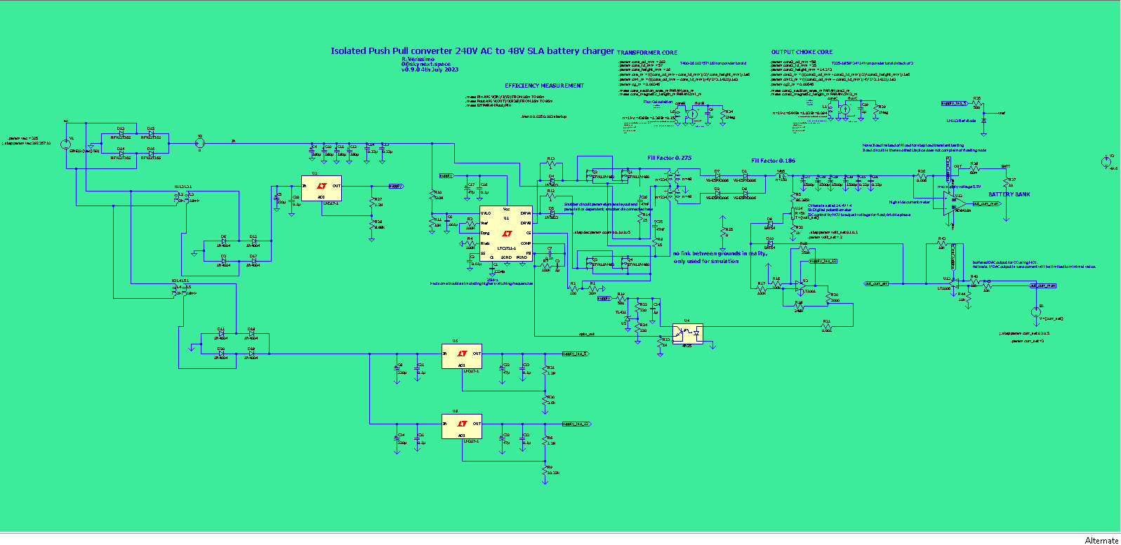
230VAC to 48V, 1400W Lead-Acid battery bank charging circuit
Model download at the end of the article
This is the complementary circuit to the 48V to 400V converter, doing the opposite conversion
However, it is presented here as a simple charger directly tied to mains without PFC.
The input line filter has been omitted for simplicity.
Since the charger assumes the presence of an AC link (230V AC for that design), logic power is supplied by two small AC/DC 50 Hz 3W transformers.
They are not modeled precisely to the specifications in this design.
The first transformer powers one LM317 regulator to provide bias voltage of 10.5V to the switching LTC3721 IC and to the optocoupler transistor. While the second transformer powers one LM317 set at 5V regulated output for the MCU, the LT1006 op-amp, and the AD8418 current metering op-amp, as well as the LM113 voltage reference diode used by the AD8418; And another LM317 with an output voltage set at 12V. The LT1001 used in the Howland current pump requires a 12V supply in order to source an adequate current level.
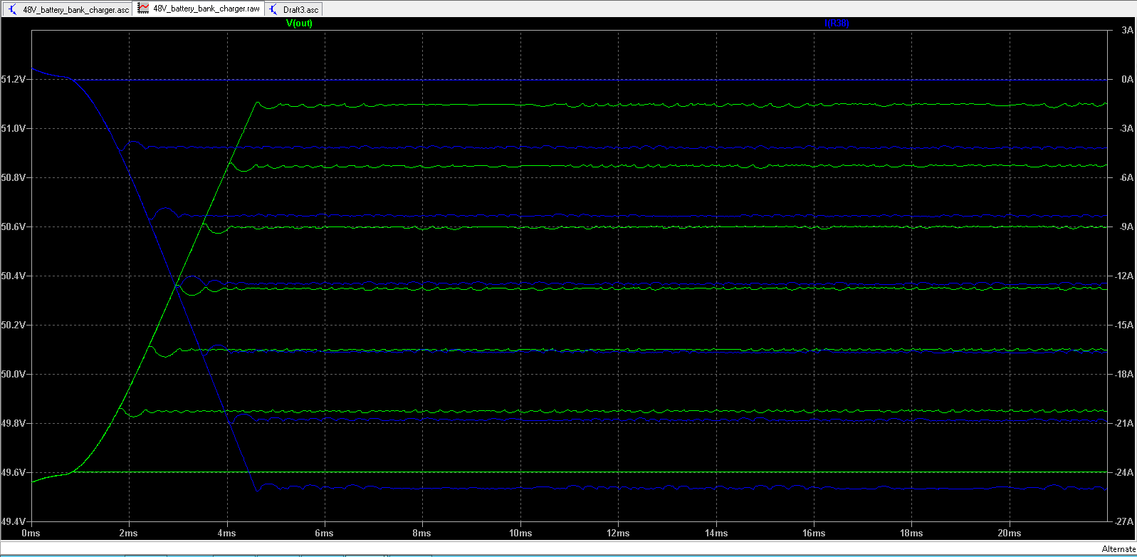
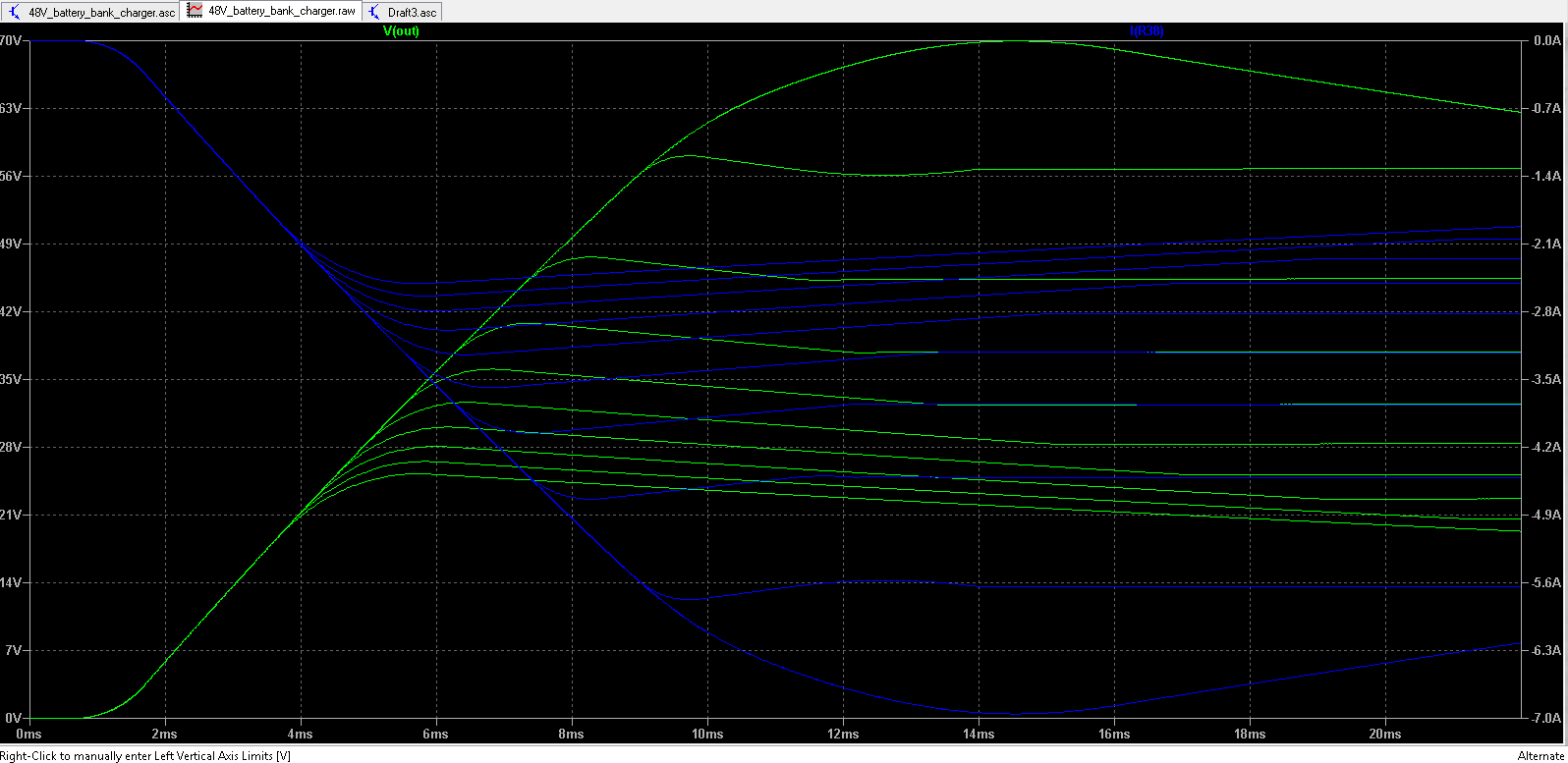
The circuit has been simulated up to 25A charging current for a 48V SLA battery bank. (Assuming an individual battery voltage of 12.4V)
Due to the simplest model used for the battery bank, the actual behavior to reach a steady state may be different.
CC is achieved by high-side current metering, whose signal is compared to a bias level output from a DAC.
The higher the DAC output level, the higher the charging current.
High-side current metering is preferred for chargers since it can detect load shorts and offers better noise immunity.
Here we use a dedicated AD8418 IC for that purpose.
This approach is failsafe in the event of a MCU failure since a 0V DAC voltage output would command a 0A charging current.
CV for float/trickle charging is achieved by varying the wiper position of a 5K I2C digital potentiometer, controlled by the MCU.
Note that the circuit has been tested on an ohmic load (10 and 25 ohm) for stability.
It could also be used as a versatile CC/CV PSU besides charging
Using the circuit as a charger for a 24V battery bank could be envisioned, but has not been tested for performance and stability at the time of publication of this article
As for the rest of the circuit, it is more or less the same as the 48V to 400V converter from the preceding post.
Due to higher output currents on the secondary, choke, the output power level has been derated.
As for stability, there is no perceivable ripple in the output up to 25A.
Assuming a charging current of 0.1*C (C being the battery capacity in Ah), This charger could theoretically charge a battery bank of four 250Ah batteries at a nominal rate.
This circuit is the simplest expression of a CC/CV charger. It does not perform a battery bank voltage check before charging, temperature compensation, or coulomb counting. These features require further MCU / digital side control and are not expected to be modeled properly in Ltspice.
Speaking of digital control, It is expected for the MCU to monitor the charging current through the AD8418 so as to set the DAC voltage “curr_offset” to perform the appropriate charging program, as well as to monitor the bank voltage, as a digital control outer loop.
Efficiencies (simulated)
Pout/Pin. Pin taken at the node after the full bridge rectifier.
| 5A | 0.951529 |
| 10A | 0.945238 |
| 15A | 0.942658 |
| 20A | 0.93861 |
| 25A | 0.933888 |
| 30A | 0.930961 |
Leave a Reply