We are currently evaluating NXP’s i.MXRT1062 CPU based MCUs as the core of our PMU-001 device.
This product is advantageous as it one of the most capable MCU in terms of raw processing power, while also featuring a FPU.
Additionally, the presence of an Ethernet module with IEEE1588 ptp functionality, gives access to an adjustable free running nanoseconds timer counter with 1 sec rollover. A robust hardware on the fly correction capability allows disciplining the counter using a pps GPS signal or an ethernet based LAN ptp clock.
Note that the additional processing power has the effect of reducing IRQ contention which may introduce jitter. Faster CPU also means availability of larger PLL scales. the cycle counter has a resolution of 1/600 Mhz, while the IEEE1588 counter timer has a resolution of 40ns
As for disciplined sampling periods, the periodic interrupt timer (PIT) period can be precisely controlled with a period correction resolution of either 1/24 Mhz or 1/150 Mhz, depending on the clock source, using the LDVAL register that affects the next period, not the current period, ensuring consistent sampling.
A simple integer accumulator and integer divider method allows distribution of corrections smaller than one period correction resolution, ensuring total correction over one second brings the IEEE1588 timestamping to a disciplined second, as well as the PIT correction that ensures a true sample rate of electrical data close to nominal.
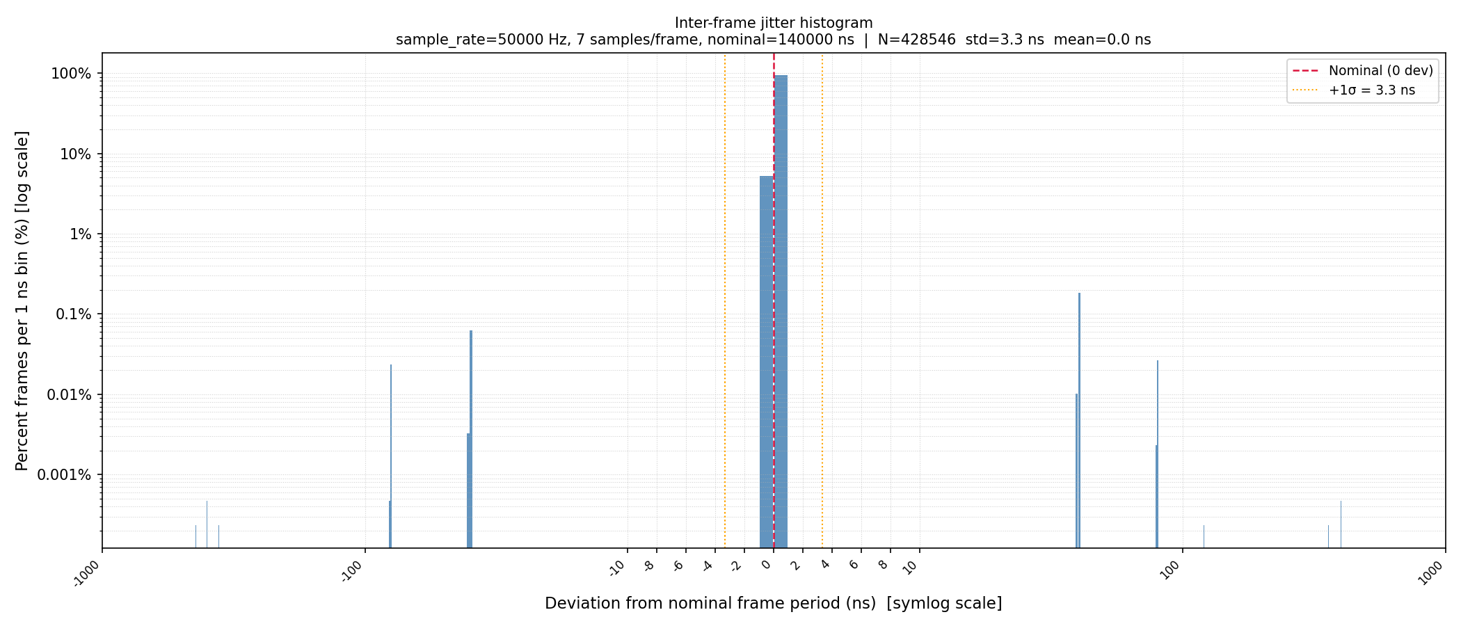
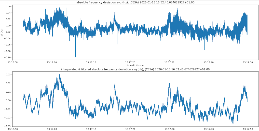
Following is the jitter analysis at 27C temperature ambient, CPU at 56C, and a 60 second recording interval of USB sample and timestamp data. No frame drops observed. The jitter analysis was performed during nominal GNSS function (no holdover).
Nominal sampling rate is 50 ksps (20 us). 8 channels recorded, 7 samples per frame, frame rate : 140 us.
symlog/log scale
As for the MCU discipline protocol : Periodic IEEE1588 timestamp timer discipline is performed every 20us sampling period, PIT timer discipline (LDVAL nominal ticks + correction) is also performed every 20us. The method used for determining the correction factor is : proportional term representing the CPU cycles phase error (absolute, not fractional error) over each pps interval, summed with an infinite integral of the residual IEEE1588 counter phase error (absolute, not fractional), also over each pps interval. Filtering of the CPU cycles phase error outliers was done by filtering out measurements above 4 sigma. The sample population maintained for average,mean and standard deviation calculations are the last 64 CPU cycles phase errors recorded (so, an history of 64 seconds)
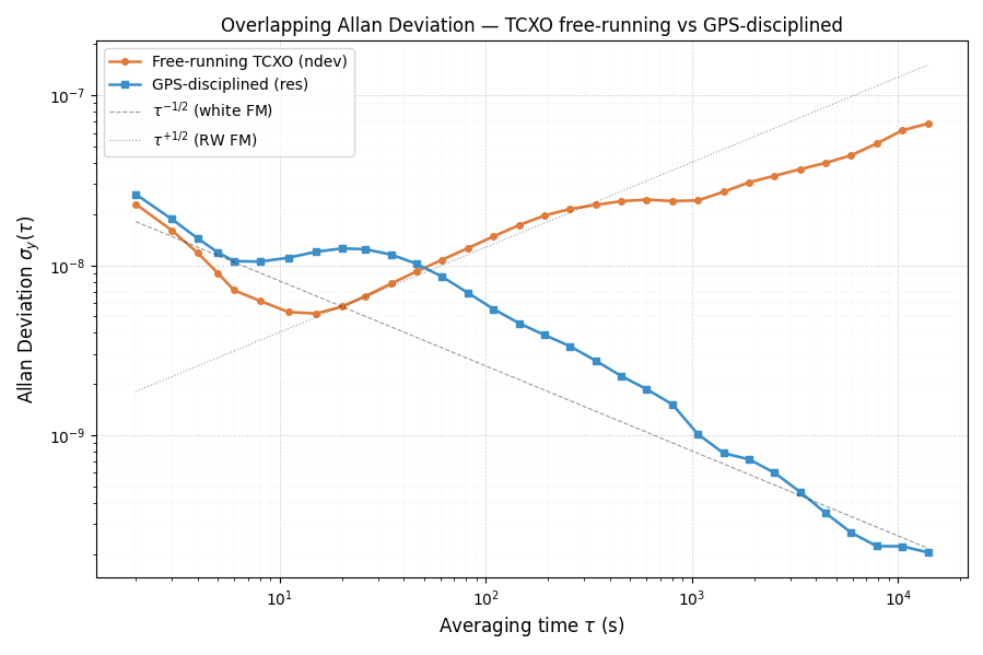
Allan Deviation chart
This is the Allan deviation calculation of the free-running CPU cycles counter, normalized to nanoseconds, and the IEEE1588 disciplined nanoseconds counter, over 41785 seconds, with a unit measurement interval tau of 1 second, while performing sampling of electrical parameters nominally at 50000 samples par second, 8 channels sampled, 7 samples * 8 channels per USB frame, and sending data over USB, but without a host listening.
We plan to perform the same measurements and Allan deviation charts without the payload calculation. Results are deemed quite satisfactory, and follow expected noise characteristics and temperature drift effects. Average temperature 45.70C @CPU, with forced convection in front of the XTAL, with CPU downstream, Average ambient temperature 25C, measurement performed at night starting at 21:30 UTC. Environment temperature is not controlled.
I will provide an updated chart with temperature data soon.
Temperature compensation
We are also evaluating an additional high precision temperature probe positioned right under the XTAL to provide ppm correction during GPS holdover intervals, with an intended goal of < 1ppm deviation during GPS holdover intervals. Such a fixture, besides providing TCXO capability without the need of replacing the onboard XTAL, also improve robustness of GPS pps signal outlier filtering, by providing ppm deviation prediction based on temperature slew, provided the temperature measurement is itself low noise. This would help identify the very infrequent but possible GPS pps glitches.
Such level of discipline precision is adequate a field microPMU, which is our intended market segment,
Discarding the requirement for an external OCXO or TCXO driven MCU or sampling timer would drastically lower R&D production, and time to market delays.
At this point in time AD7606 interfacing has been done on the new MCU platform with satisfying results.
Thus, We are now moving our development efforts towards PCB design.
For more information about i.MX-RT1060 and i.MX-RT1062 based MCUs :
Rework and Refactoring of the Host based PMU logic
We are currently in the process of updating our host based code to improve overall performance and add a substantial margin of processing time taking into account all PMU P-class and M-class modes and reporting rates, So as to deliver a product that is adequate to a large segment of cost effective and available SoC platforms, and ensuring device form factor compliance for size restricted cabinets and challenging thermal environments. This should not alter significantly the mentioned December 2026 deadline for a commercially adequate product delivery.
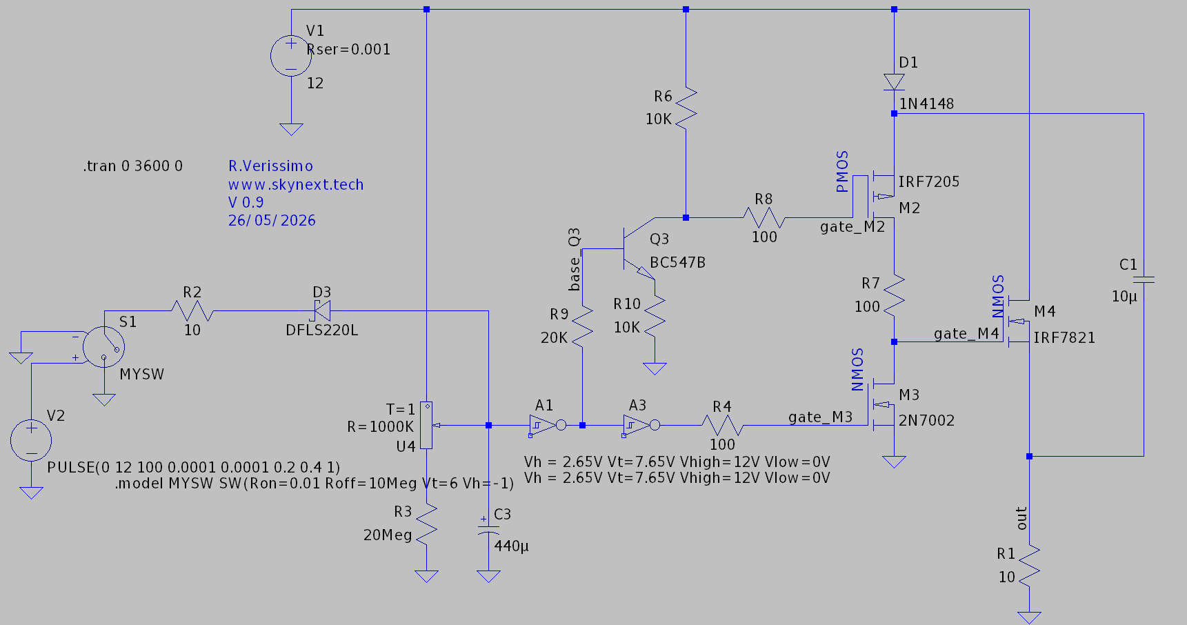
When it comes to switching timer modules, most designs are either based on the good old 555 timer, or some kind of 8 bit MCU that performs supervisory functions (like turning a relay off and keeping track of time), with the advantage for the later to allow for various timing and delay on/off programs. Most designs however, draw hundreds of microamperes up to several milliamperes while idling. Since one common use of these timers is to power a load for a given time in off grids setups where stored battery energy must be conserved, a low quiescent current solution would be a preferable design. Most designs are also relay based. Sturdy relays have an advantage of providing NC/NO modes natively, tolerate inductive kickback from loads such as motors, and are immune to spurious turn-ons.
Here we present a fully solid state timer delay off high side NMOS switch, thus with low Rds ON. The power to the load is turned on through a pulse (such as one supplied by a spring loaded pushbutton), latches, and turns off based on the timing constant of a RC network.
Giving the maximum rating of the CD40106 Schmitt trigger used here, the maximum switched voltage is around 18V. A higher voltage rated Schmitt trigger inverter would allow 24V operation, and using MOSFET rated above Vds of 30V would push operation voltages into 48V or more.
The transient connection of the switch S1 discharges the capacitor C3 through D3 to ground, bringing temporarily the schmitt trigger input to ground potential. output of the trigger goes to logic 0V, while the inverting input goes to logic high. A CD40106 schmitt trigger can be used to implement complementary outputs, by daisy chaining two stages as shown in the schematic (A1 and A3). The operational parameters of the CD40106 at 12V have been calculated from the datasheet and added to the model.
In the low voltage state, the first inverting output of the schmitt trigger A1 is in logic high, sinking current into Q3 base, which has the effect to lower gate potential of PMOS M2, turning it on, and supplying bootstrap capacitor voltage to M4, which turns it on and performs the intended high side switching function, While schmitt trigger A3 output voltage goes 0V, turning M3 firmly off and preventing fast discharge of C1.
When the RC network charges back above Vhigh threshold, M2 is turned off, which has the effect of stopping the supply of voltage from the bootstrap capacitor to M4, and bringing the gate of M4 to ground through the turn on of M3. This effectively turns off M4.
Giving the low gate charge and leak of modern NMOS, the bootstrap capacitor C1 can supply voltage to the gate of M4 over a time far longer than the time constant of the RC network made with U4 + R3 and C3.
Note that M2 does not handle large currents in that circuit. A smaller footprint PMOS could be used, rated for logic Vgs levels (such as -5V)
Note that the transition Vhigh and Vlow voltage of the CD40106 used are linear functions of supply voltage, Which means that a higher or lower Vcc operation as supplied from a battery should not change the minimum and maximum delays achieveable significantly.
Resistor R7 acts as a current limiting resistor for gate current but also during switching of M2 and M3, which could temporarily provide a low impedance path to ground. Note that CD40106 propagation delay using two stages in a daisy chain have the effect of introducing a small dead time between M2 and M3 switching, thus mitigating that unwanted effect.
This is a quick update on our flagship product development, PMU-001. Since October 2024, we put great effort in developing it. The PMU-001 USB device is intended for electricians that need a portable and reasonably affordable field device which provides the following features :
Robust GNSS based synchrophasor measurement, IEEE Std C37.118-2005 compliant with network bindings.
6 channel analysis (3 voltage channels, 3 current channels, 2 auxiliary channels)
4 quadrant power analysis
Positive, negative and zero sequence vector decomposition
logging and real-time (within standard delay requirement) equispaced sampling of frequency deviation from nominal mains
Harmonics analysis and THD display and logging
waveform logging
USB 2.0 high speed device, hardware sampling rate 48 ksps.
Lightweight NCURSES interface allowing use across low speed / character based tty
Integrated class 0.1 voltage measurement transformers with secondary DAC TVS protection / clamping on top of internal DAC protection.
1000V AC transformer winding voltage tolerance.
Line to Line or Line to Neutral voltage measurements (120V up to 240V AC / 208V AC to 400V AC nominal voltage +15% tolerance)
It leverages the power of a personal computer for high level analysis, reducing hardware costs, the software payload is C++ based and works on Linux distributions. Microsoft Windows porting is planned in the future.
A fully functional hardware and software prototype is planned for Q3 2026.
Most of the work is now dedicated on GPS disciplining and TCXO clocking, as well as cross channel analysis for four quadrant measurement, and delay vs filtering efficiency real time tuning. IEEE Std C37.118-2005 compliance will require rigorous conformity testing and calibration. At that time, a crowdfunding effort with pre-order priority will be put into effect, allowing trade electricians to have priority access to the device in the beta phase.
Here are some video and screen capture teasers :
NCURSES display of frequency deviation, ROCOF, harmonic analysis, amplitude analysis, and synchrophasor data. Single phase to neutral display.top chart : raw frequency deviation measurements at 100 Hz sampling rate; bottom chart LP filtered at 10 Hz cutoff frequency and PCHIP interpolated/equispaced frequency deviation measurements. Network PMU connection to PMU-001 using GPA PMU Connection Tester tool, displaying a single voltage channel synchrophasor and frequency measurements.Websocket synchrophasor and frequency deviation interface (alpha version)
We wish everyone a fruitful 2026 year. Stay tuned for updates !
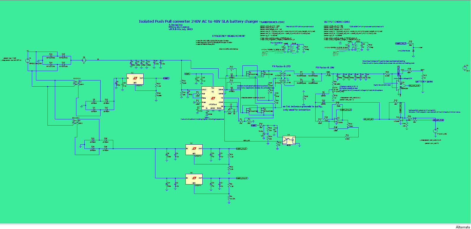
This is the complementary circuit to the 48V to 400V converter, doing the opposite conversion
However, it is presented here as a simple charger directly tied to mains without PFC. The input line filter has been omitted for simplicity.
Since the charger assumes the presence of an AC link (230V AC for that design), logic power is supplied by two small AC/DC 50 Hz 3W transformers.
They are not modeled precisely to the specifications in this design.
The first transformer powers one LM317 regulator to provide bias voltage of 10.5V to the switching LTC3721 IC and to the optocoupler transistor. While the second transformer powers one LM317 set at 5V regulated output for the MCU, the LT1006 op-amp, and the AD8418 current metering op-amp, as well as the LM113 voltage reference diode used by the AD8418; And another LM317 with an output voltage set at 12V. The LT1001 used in the Howland current pump requires a 12V supply in order to source an adequate current level.
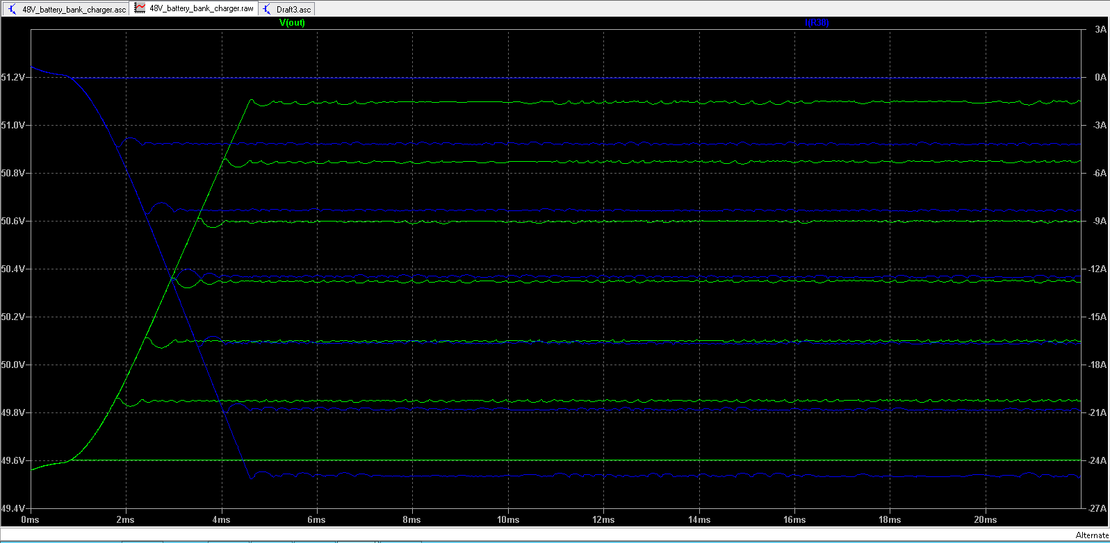
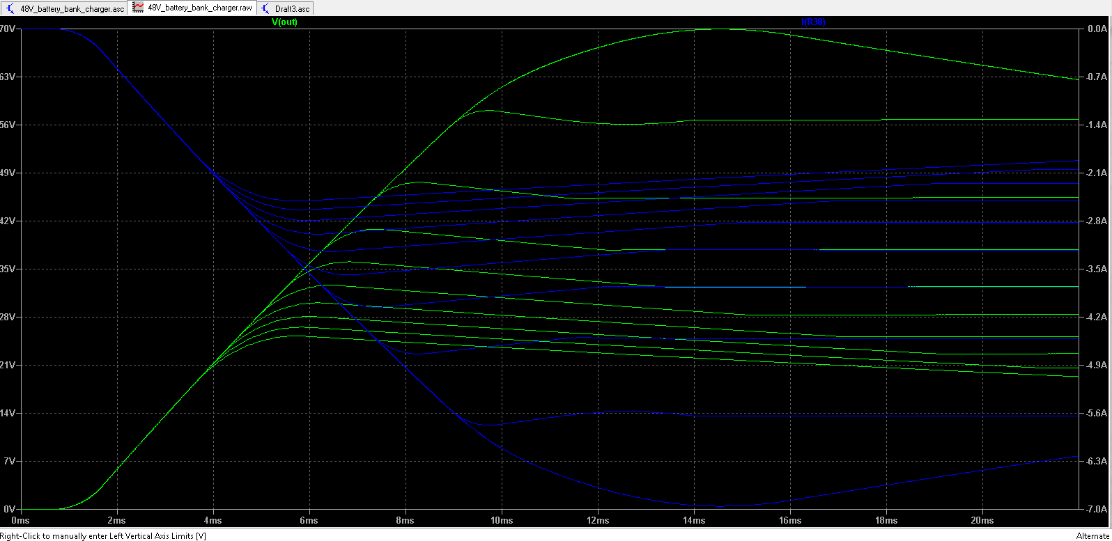
The circuit has been simulated up to 25A charging current for a 48V SLA battery bank. (Assuming an individual battery voltage of 12.4V)
Due to the simplest model used for the battery bank, the actual behavior to reach a steady state may be different. CC is achieved by high-side current metering, whose signal is compared to a bias level output from a DAC. The higher the DAC output level, the higher the charging current.
High-side current metering is preferred for chargers since it can detect load shorts and offers better noise immunity. Here we use a dedicated AD8418 IC for that purpose.
This approach is failsafe in the event of a MCU failure since a 0V DAC voltage output would command a 0A charging current. CV for float/trickle charging is achieved by varying the wiper position of a 5K I2C digital potentiometer, controlled by the MCU.
Note that the circuit has been tested on an ohmic load (10 and 25 ohm) for stability.
It could also be used as a versatile CC/CV PSU besides charging
Using the circuit as a charger for a 24V battery bank could be envisioned, but has not been tested for performance and stability at the time of publication of this article
As for the rest of the circuit, it is more or less the same as the 48V to 400V converter from the preceding post. Due to higher output currents on the secondary, choke, the output power level has been derated.
As for stability, there is no perceivable ripple in the output up to 25A.
Assuming a charging current of 0.1*C (C being the battery capacity in Ah), This charger could theoretically charge a battery bank of four 250Ah batteries at a nominal rate.
This circuit is the simplest expression of a CC/CV charger. It does not perform a battery bank voltage check before charging, temperature compensation, or coulomb counting. These features require further MCU / digital side control and are not expected to be modeled properly in Ltspice.
Speaking of digital control, It is expected for the MCU to monitor the charging current through the AD8418 so as to set the DAC voltage “curr_offset” to perform the appropriate charging program, as well as to monitor the bank voltage, as a digital control outer loop.
Efficiencies (simulated)
Pout/Pin. Pin taken at the node after the full bridge rectifier.
The following design comes with no guarantees whatsoever. Although a decent amount of time has been spent to ensure that the model works well over the whole range of its design constraints, some errors may still linger, Some more experienced engineers may find some design choices questionable, If you’re able to optimize it or build something better around it, that’s nice.
The choke inductor and the transformer may be a little over-engineered and drive the costs up, given the large ferrite core choices.
You may be able to extract more power than 1600W, but tread carefully.
Additional Resources :
The download is available at the end of this article.
There is also the ‘sister project’ to this one, which performs 230V AC to 48V DC conversion, with the intent of battery charging : It is designed to allow current/voltage control via DAC and a digital potentiometer, so you can digitally control voltage and current and design a charging program.
The main goal of this model is to serve as an aid in learning about the Push pull converter topology, it also could prove useful when building a prototype, as a part of a UPS or solar converter design.
Care has been taken not to overburden the simulator and allow reasonable simulation speeds.
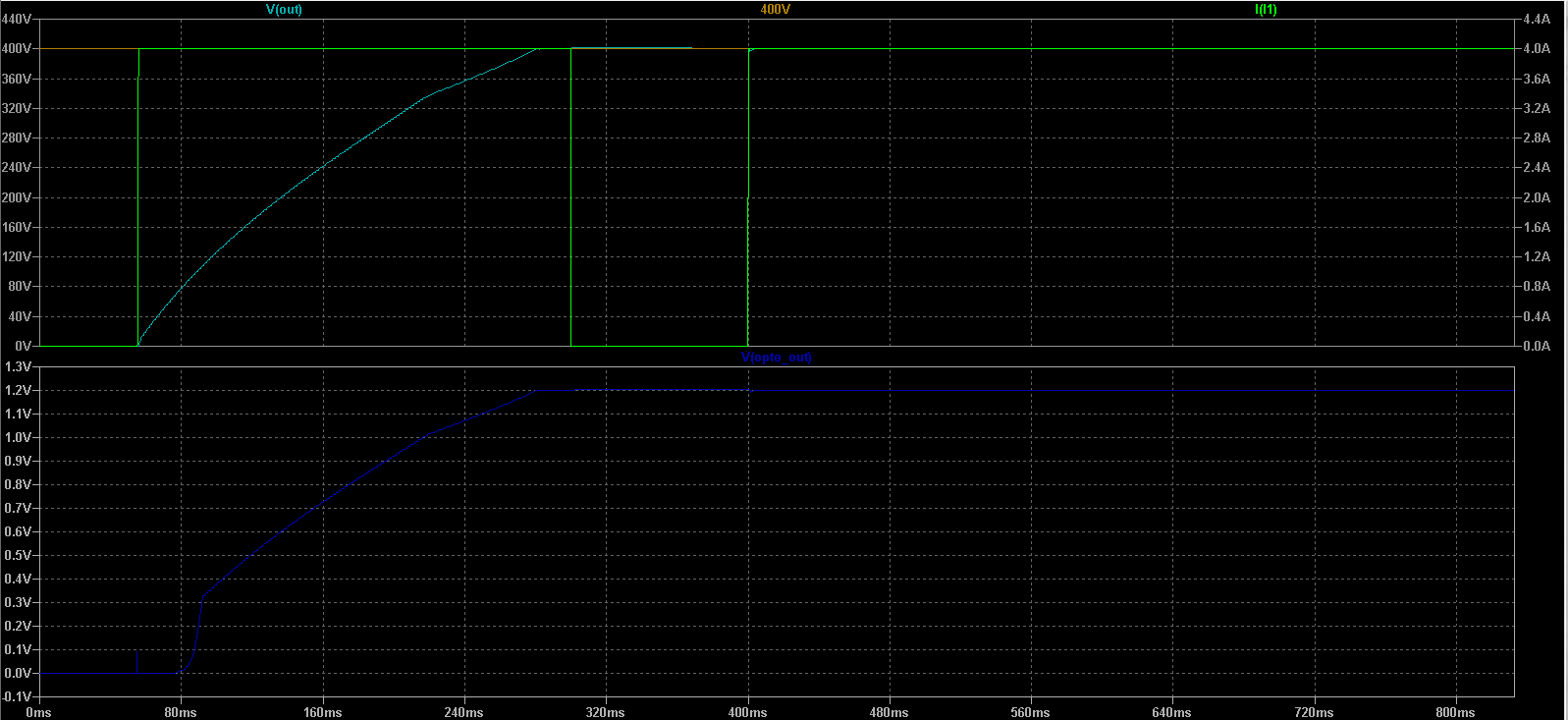
Most of the simulation time is spent ramping up the voltage (soft start) Using smaller starting loads and stepping them once the converter is fully started decreases simulation time, Once you’ve determined that the soft start ramp is ok.
Intended Audience:
Makers or junior power engineers with little experience, looking for a project that can lead to prototype build.
Three models are supplied :
The fastest one uses linear inductors, voltage sources for IC power, no isolation, and a simple feedback circuit without optocoupler isolation.
The second one is the same as the model above but with non-linear inductors (Chan model)
The full model uses proper and more realistic component DC supply schemes as well as non-linear inductors, as well as isolation. Note that Ltspice is not always able to process isolated secondary circuits, even with the use of a stitching resistor, unless it is very low resistance. Here the problem appeared so we linked both grounds. A practical circuit, of course, will not have that constraint.
Design Parameters
Max continuous power, 1600W max. Inductor Thermal effects are not modeled, derating may be advisable, Although a large saturation margin has been taken into account.
Input from 48V (discharged battery, UVLO threshold) up to 57.6 (bulk charging voltage when a charger is connected)
400V DC output. it supplies the same voltage as a PFC would.
This allows easier load switching or load sharing between the battery source and the AC / PFC source converter and can be adapted to larger designs.
Optimized for high power.
Moderate to good efficiency 0.93
Low cost. (uses powder core inductors)
Fully isolated design.
Under Voltage lock-out set at 48V to prevent battery bank over-discharge
4mm² wire for primary of transformer, 2*24 turns, center tapped
1.5m² wire for secondary of transformer 2*234 turns, center tapped
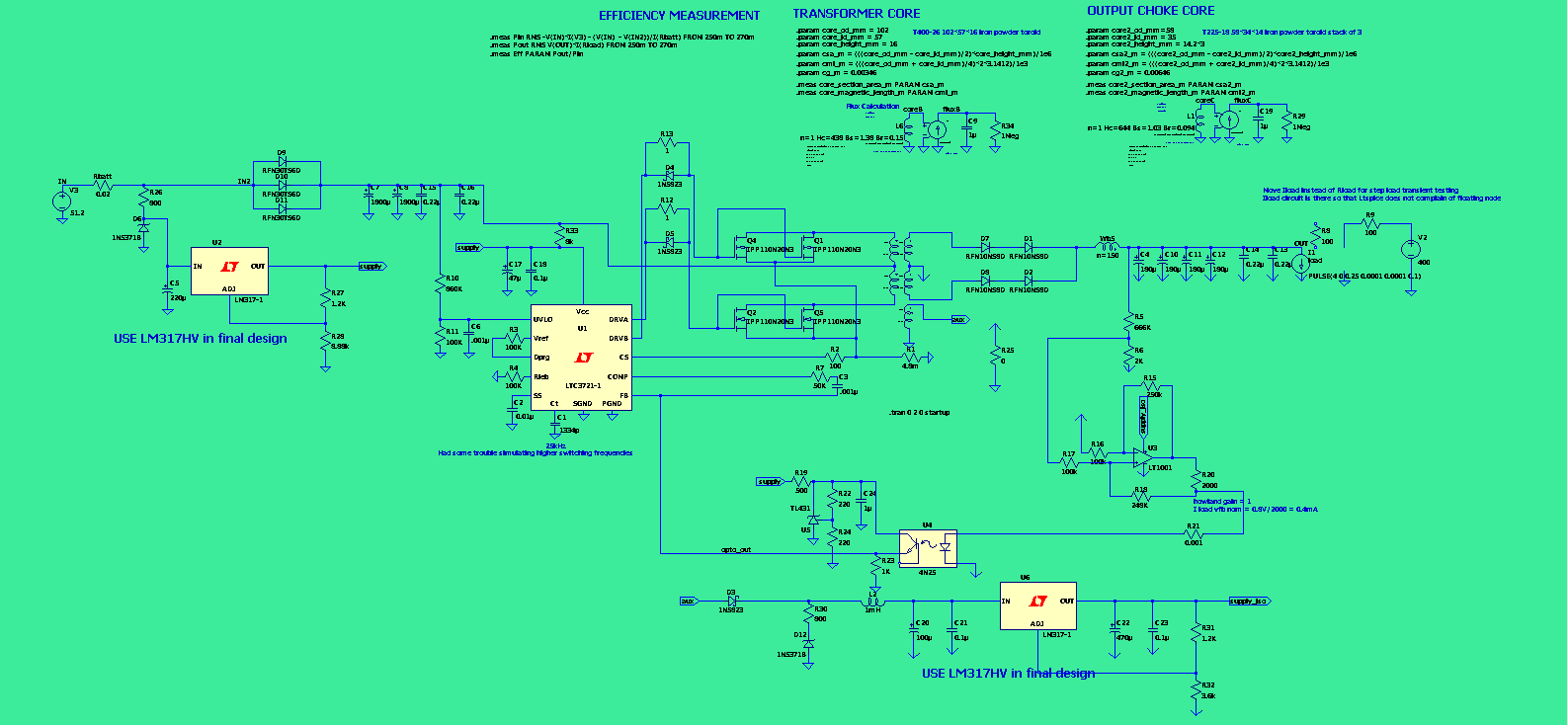
T400-26 transformer core (Iron powder)
As said before, it is for teaching or training rather than commercial purposes. It will require hand winding of the toroid to build a prototype. (which is a cumbersome and long process, It is advised to watch several videos about that art to do it properly the first time. (You do not want to rewind it a second time). Building a toroidal transformer is a valuable learning experience.
Some Toroid Winding tips :
Use proper dielectric insulation between windings to control parasitics, it also serves to protect the windings from abrasion.
Use a counter to keep track of turns.
Keep the winding tensioned so it does not spring back. You can also ask toroidal transformer shops to build you a custom transformer according to your specifications. Proper care has to be taken to balance the primary windings around the center tap as equally as possible to avoid flux imbalance. Fortunately, the number of turns of the primary is low.
Strategically place the tap halfway through the core height, and wind the primary legs as symmetrically as possible, by adequately controlling the winding pitch. Looking at resources explaining the proper way of transformer tapping is advised.
To make enamel wire solderable, I usually use abrasive dremel cylindrical tips. Do not use a flame as the enamel is very flame resistant and that will anneal the copper making it more fragile.
You can also watch videos from HAM radio makers, as a lot of them have mastered the art of core winding. A balun is not exactly the same as a push-pull transformer, but a lot of practical building tips apply.
Always check the final product inductance while testing on exposed wires, with a margin of excess wires so that you can always add turns if inductance falls short. Fortunately, transformer inductance is not that critical, what is critical is balancing and the turn ratio.
Note that It will be hard to find an exact turn ratio from commercial solution catalogs, but you can always look for and adapt the design accordingly. A different ratio will affect the minimum and maximum duty cycles of the converter which could make achieving the 400V target harder at the nominal output load of 4A.
Capacitor Considerations
Input capacitors do not need to be large because of the low battery impedance and stable voltage.
Output capacitors should be low ESR, We choose expensive high capacity, high-voltage electrolytic capacitors to maximize hold time and for lower ripple, and to make the choke sizing reasonable.
Hold time considerations mostly depend on the load parameters Additional 450V MPP film capacitors were used. Do not use X2 line capacitors as they are designed to fail short.
MOSFET considerations.
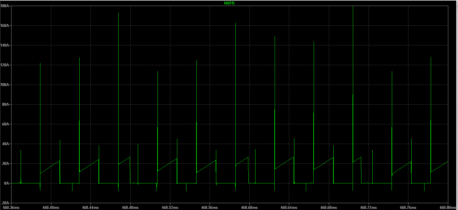
In our design, each MOSFET is subjected to 25 A average current with peaks of up to 120 A due to parasitics (at turn-on), with low-value gate stoppers resistors.
Infineon’s IPP110N20N3 are rated at Id of 88 A and pulses up to 352A. The datasheet is available at :
Thermal management of MOSFET is of utmost importance a clever prototyping solution could make use of radiator/fan bundles designed for CPU cooling, as they often integrate heat pipes, This would complicate the layout significantly and the total prototype volume because of the sheer bulkiness of these kind of components, and require drilling the heatsink backplate. A single modern and standard CPU heatsink fan can cool loads of around 100W. Calculate maximum MOSFET losses and design the solution accordingly.
Never operate MOSFETs under load without proper thermal management!
Overcurrent Protection.
The Switching IC provides a hard current limit that stops switching in case of overcurrent and a resume algorithm explained in the datasheet. For soft current limiting and output CC, you’ll have to implement a current monitor yourself and a feedback signal that overrides the CV signal fed to the optocoupler in case of an overcurrent situation that would decrease output voltage.
Inductance range tolerance is high since the push-pull converter is based on transformer action. It is not a critical design parameter.
The allowable duty cycle range will dictate the maximum voltage differential between the primary and secondary, in combination with the output voltage range. The fact that the input could already be thought of as regulated (it is a battery, but may be subjected to higher voltages seen by the converter during charging) and that the output voltage is designed to be kept constant eases the design. It is however important not to drive the core into saturation, So we have made the choice of a large T400-26 iron powder core, although thermal effects (and the decrease of inductance caused by it, will play the limiting role rather than saturation. Here the margin is <add figure> A larger core also allows a lower fill factor which will improve cooling and reduce ohmic heating from the current flowing into the conductors. It also makes manual construction easier. As said before Controlling the winding balance in the primary is critical in Push Pull converters. An imbalance gives rise to a Bias flux buildup that decreases efficiency.
A low fill factor also allows better cooling performance, even more so if forced (fan) cooling is used to blow axially through the core. When building a transformer, optimization is complex because of the large parameter domain.
For such a design, it is advised to perform a faster simulation using a standard LTspice coupled inductor,, and specify coupled linear inductors inductance based on Push Pull converter design formulas, and check that the circuit performs ok on that basis. taking care efficiency changes into account with each parameter changes, and performing load stepping, and voltage input range stepping. Efficiency should be high using a fully linear transformer. If not, something is amiss. Remember that efficiency also depends on load, and is usually lower at very light loads.
On the basis of this first design iteration look at the current flowing through the primary (RMS and peak values), and knowing the number of turns you’ll get the H field strength, which will be used to get the B field strength. B = H/(µo*µr) Then you can look at material tables and check that you are operating within a safe margin. It is a bit complex because there are derating factors, for instance, because of frequency.
Thermal runaway is the situation you want to absolutely avoid (It decreases inductance, which increases the magnetizing current, making the core saturate even more and induces losses which translate into thermal runaway) Our strategy is low-cost-driven. We choose low permeability iron core and decreased switching frequency to minimize core losses. (iron powder cores perform better at lower switching frequencies) Iron powder cores are low permeability because of the distributed air gap between magnetic particles, and exhibit high (around 1.5 T) and soft saturation. For the main transformer, we choose the low-cost 26 Material, and selected a large T400-26 core, allowing higher fill factors. The transformer turn ratio requires a large turn number for the secondary. For the output choke, we used a lower permeability 18 Material and a quite large stacked core. Output inductors/chokes operate at a high current bias level so that it derates inductance. Inductance value is also a critical design parameter. When using a suboptimal (too low inductance, output ripple, and inductor heating will be higher, with also a risk of thermal runaway and gradually decreasing stability.) We noted that when using too low inductances, the design refused to reach our target voltage, Which seems to be a protection feature of the converter IC.
To sum up, We have to obtain an inductance large enough for our filtering goals at nominal power while reducing the bias B field. B field is proportional to the number of turns times permeability, all other parameters being equal, while inductance increases with the square of the number of turns times permeability. Thus it follows to use a larger core with lower permeability to accommodate a larger number of turns to meet inductance requirements while staying under saturation levels. To lower the B field, we also used the stacking strategy to increase the total compound core area. It is easier to wind that way than individually winding inductors and placing them in series, on the board, especially if PCB real estate is a concern. It would however decrease cooling efficiency. Not seen much about that method in commercial products, as it could also increase flux leakage. Better test it.
EMI concerns.
The low-frequency operation of 25Khz reduces EMI concerns depending on regulations on that VLF band and the other components that may be subjected to it. It is above the audio hearing range, but some harmonics may find their way into audio equipment (The IC switching frequency may go up to 1Mhz, changing the frequency would require choosing a better-suited, ferrite instead of iron powder material and adapting core dimensions, usually smaller ones. However, we had trouble making the simulation run smoothly at higher switching frequencies. Higher switching frequency also has a dramatic impact on simulation performance, as the minimum timestep has to be lower.
Of course, general layout guidelines apply, such as reducing the loop area of switching components traces paths (MOSFET drain to source) and the length of gate signals. Shielding is an option if it does not interfere with cooling.
Lower frequency however could make the core produce an audible stridulation effect, because of the magnetostrictive effect that is close to the audible range.
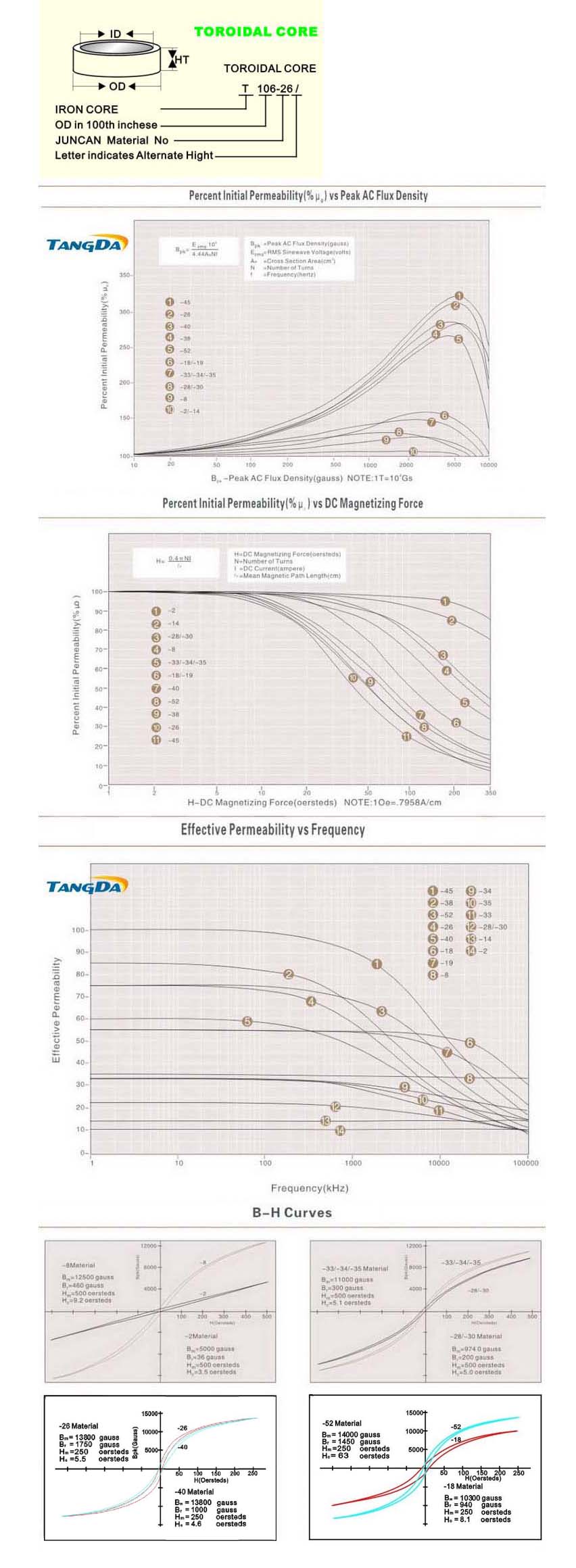
Core design helpers :
Our advice is to use a Ltspice core test bench using the resources here : https://www.eevblog.com/forum/projects/arbitrary-%28saturable%29-coupled-inductors-in-ltspice/
Magnetics catalogs and materials datasheets from major Western manufacturers: TDK Epcos, Ferroxcube, Magnetics.inc Micrometals,
The same for Asian ones: JUNCAN, Tangda, Caracol, etc… A popular seller is Tangda if you need to source (relatively) cheap cores from China.
The B/H curves when you can find them, if the Chan model parameters are not specified.
Magnetics cross-reference lists, images and pdfs. This will make selecting cores a littles easier, when switching from one manufacturer to another.
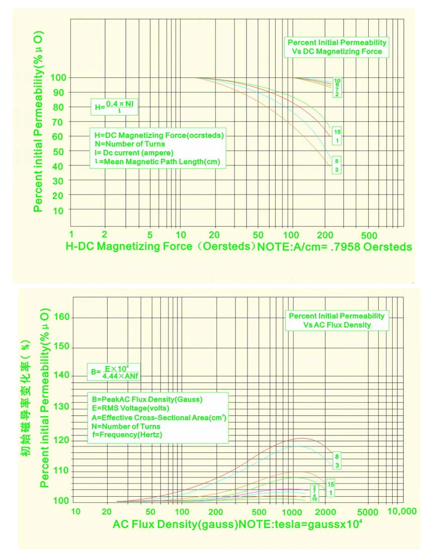
If you need to look at a B/H curve or if you have experimental data from a B/H curve tester (usually pluggable to an oscilloscope), you will need to find the crossing points on :
the B axis (y) : for Br (B field – remnant) and Bs (B field – saturation)
and the H axis (x): for Hc (H field – coercivity).
Bs is the saturation (horizontal asymptote line B value) for hard saturation, for soft saturation it is determined differently, as the B field keeps increasing, albeit with a lower and lower slope.
A good rule of thumb for soft materials is to stay in the linear region, with a good (30 to 40% margin)
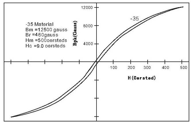
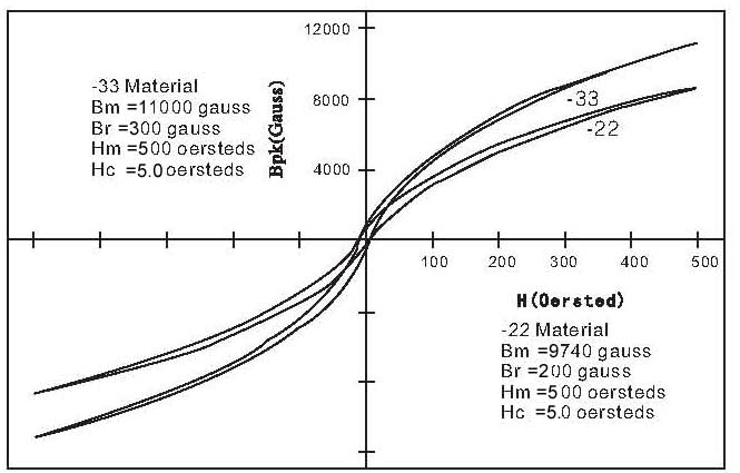
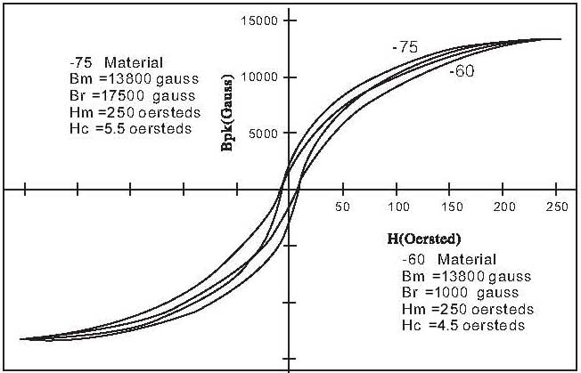
Fortunately, Chinese manufacturers provide the B/H curves and Br, Bs, and Hc.
With all these collected data, you are ready to test the cores in the Ltspice Chan model test Bench.
Use the manufacturer-supplied geometric data OD, ID, and Height. We updated the test bench with geometric data calculators for the magnetic length and area required by the model.
Input magnetic data for the Chan model, taking care to use SI units: Hc (A/M), Br (T), Bs (T), (Amperes/m and Tesla)
Alas, Western Manufacturers usually provide the Al value and Bs (B sat) but almost never an exploitable full BH curve. You will need to contact them for this, but it may be a trade secret, who knows?
What you can do however is parse scientific publications to get harder to find values such as Hc and Br, and the problem is that they come for generic alloys (says MnZn, or very exotic ones) A comprehensive database of core parameters is clearly needed at this point.
If the data is in Oersted and Gauss, multiply the Oersted value by 79 to get A/m and for Gauss divide by 10000 to get Tesla units.
Some reference data, mostly for iron core materials collected that you may find useful :
An important note that I have not confirmed at this point: Note that the Iron powder materials data found on Chinese resellers are (presumably) for a pure (no distributed gap) material, thus if you plug the data into the mag_inc_bias.asc, you’ll find an abnormally large Al value.
So the strategy is to set primary_turn in the test bench model at 1, and play around with the core Chan model parameter Lg (gap length value in meter), until you obtain the nH/t^2 that is specific to the core.
Remember to set I_bias to 0. There is also a 60nH inductor in series, that would need to be set to 0 for adequate measurements of very small inductances.. I have no idea what is the purpose of this.
SUMMARY OF INDUCTOR TEST BENCH SETUP
Create one asc file based on mag_inc_bias for each core (makes life easier)
Fill in geometric data
Fill in material data (Hc, Br, Bs)
Set primary_turn to 1.
Set I_bias to 0.
Find distributed air gap equivalent gap length L_g by trial and error (examine inductance .meas in the error log) until the inductance value is equal to datasheet Al.
This is particularly useful to test for inductance decrease due to I bias current (seen in the output inductor choke) If you need to lower the testing frequency, you’ll need to increase the simulation time because the measurements use 15th/16th cycles of RISE/FALL for inductance measurements, otherwise, you’ll get “measurement failed”
Inductance measurements are required for the choke, for the transformer, just check that the B field remains under Bsat with some margin.
Note that the I1 source is used for inductance measurements (It is set at 1mA, thus the x1000 factor in inductance measurement) The measurement is based on the formula V = Ldi/dt, L = V(dt/di) = V/freq2pi at zero cross.
Increasing I2 will decrease inductance This is used for the choke measurement (under DC bias). Test with I2 value equal to the max allowable output current, with the frequency set correctly and the choke turn number set correctly. Verify that the inductance value is still above requirements and that the B field in Tesla is not above Bsat.
As a final note, It should be said that the Chan model has been superseded by the Jiles-Atherton model which shows better fidelity to the experimental BH curves. Unfortunately, Ltspice models using the JA model (CoreJA) are prohibitively slow for use in power product simulations, But the test bench could be adapted using CoreJA. The advantage of the Jiles Atherton model is that you can find a database of JA parameters for a lot of cores in the magnetic.txt file of the ZZZ library. This is the famous Bordodynov library (also known as the Yahoo Ltspice group library or the Ltspice groups.io library) It is a must for every serious Ltspice user.
Software also exist that help in complete solution design with an emphasis on magnetics, such as ‘ExcellentIT’, and also good product finders on manufacturer’s websites, to help in core selection.
Once you have made a provisional choice for the cores, turn number and turn ratio, you can replace the linear models using inductances with the Chan model using the turn number. The Chan model slows the simulation speed only very moderately.
Isolation
This is an isolated design, However, Ltspice complains when using separate grounds, unless stitched by very low resistors. here we used a 0 ohm resistor between GND (primary ground) and COM (secondary ground) in practice of course there is galvanic isolation.
Optocoupler tuning
We used a TL431 to provide a stable 5V reference required by the optocoupler output transistor. To provide current to the optocoupler diode we use a modified (improved) Howland current pump.
Using a simple shunt resistor of around 240k to control the current flowing into the diode induces noise in the simulation. It should be tested in practice. The advantage is that such a solution would be passive and not require a low-voltage DC supply operating on the isolated side.
Replace the passive resistor load with an active load (flagged as load) The compensation network can be tested for stability by stepping the active load, and examination of the induced voltage oscillatory response, its amplitude, and its damping characteristics.
Ltspice (the latest version) also offers transient frequency response analysis. It combines transient analysis (so that the circuit operates normally), while a small signal stimulus is provided on the input voltage side. The small signal response on the output is analyzed so that a Bode Plot can be drawn and analyzed for stability. (checking gain margin and phase margin taking into account the switching frequency vs the frequency location of poles and zeros.)
Combining frequency analysis with a transient analysis has the advantage of not requiring specialized frequency response models for IC (When they are available) In this model, the input voltage is stable, Output capacitance is large with a low ESR, which helps for stability. A good test would be to introduce a disturbance by simulating a charging operation in the bulk (constant current) charging phase.
Powering up the IC, the Optocoupler, and the current source OpAmp
The switching IC has access to the primary side power battery power. As it is a well-behaved supply, no need to power the IC from an auxiliary winding from the main transformer. Powering the IC is documented well on the IC datasheet. In our case, however, the design is simpler.
Note however the presence of the R33 resistors that shunts some current from the primary DC link into the IC, charging the capacitor faster, than what the LM317 alone would do, and allowing the IC to start faster, The datasheet uses a 2k value for ar 12V primary, we just scaled it linearly. In this design, we used a simple LM317 regulator, which may be used to power other logic loads. The LM317HV version tolerates the battery bank voltage. You can also use a lower voltage version and power it from a single battery unit closest to ground, Which would have its positive terminal sitting at 12V above primary ground. Note that the IC is internally regulated at 10.5V or so, and can operate as per datasheet with as little as 8V. We found that it needs 10.5V during startup, and we set up the LM317 to supply a constant 10.5V. The absolute maximum rating is 12V. We also used a pre-regulator high voltage 60V Zener to protect the LM317 in case of a voltage transient. (Which could come from the charging operations)
For the secondary, things are a bit more complicated. The only active component here is the OpAmp of the Howland current pump driving the LED of the optocoupler. In reality, it is almost guaranteed that other logic or control components will be operated at low voltage with a secondary ground reference. Thus we used a 5V setting for the secondary side LM317, This low voltage did not seem to affect negatively the operation of the Howland current pump opamp
We could assume that the 400V link always has access to power, for instance, a rectified mains AC power source output from a 400V PFC unit. In UPS and solar applications, that may not be always the case, take as an example the “cold start” of an UPS from the battery in the absence of mains power.
The absence of power to this component means no voltage feedback signal to the switching IC. It needs to power up quite fast (well before the secondary reaches 400V DC) For this, we use a secondary auxiliary winding, a rectifying diode, and an LM317 set up for 5V output to power the OpAmp. The LT1001 Op-amp. is fully turned on at around 2.5V
An optional Zener could be added as a TVS function to clip transients above the LM317 rating.
MOSFET parasitics, ringing, and leading-edge current spikes.
Figure 4 shows leading edge current spikes, they are not associated with ringing (as they are fully damped). The following thread identifies the culprit as being the reverse recovery time of the secondary side rectifying diode as well as the gate pulse. To minimize these effects, One can use fast recovery diodes for the secondary rectifier, as well as to increase the gate stopper resistor values (but the latter has drawbacks, as we’ll see in a moment). Reducing these spikes by using fast recovery diodes may increase overall efficiency, as well as decrease HF EMI (the spike frequency is substantially higher than the switching frequency).
In our simulation, the current spikes are well under the 352A max pulse current specification of the MOSFET, so it should not damage the MOSFET over the long term. (When using standard silicon diodes for the secondary’s rectifying diodes.
Although this model does not exhibit this unwanted phenomenon, it is probable that a real-life implementation would because of parasitics that are not modeled here.
Ringing comes from MOSFET parasitic capacitance, coupled with the driven circuit (a transformer) inductance as well as trace inductance. Most of the push-pull converter designs come with some sort of snubber (RC series circuit across drain and source, tuned to the problematic ringing frequency), However, Value tuning is quite layout dependent. Having broad but short gate traces also helps in the management of the problem. make sure your layout accommodates some room to add a snubber.
A resistor gate stopper (here 1 ohm) also may help, but its value cannot be pushed too high: You also have to take into account gate capacitance. A large gate capacitance cannot suffer from a too-large gate stopper resistor, or the MOSFET will turn on slowly, and the slow turn-on will increase average Rds. On the other hand, a too-low gate stopper could push the gate currents above the IC specifications, especially if the MOSFET gate capacitance is high. (Which is somewhat the case for high-power MOSFETs) Thus a snubber seems like a good option.
Remember that this part may exhibit different behavior in real life due to the non-modeling of all parasitic effects and their layout dependence.
Using a 4-ohm resistor instead of 1 ohm decreases the peak pulse current from 210 A to around 160 A.
Figures
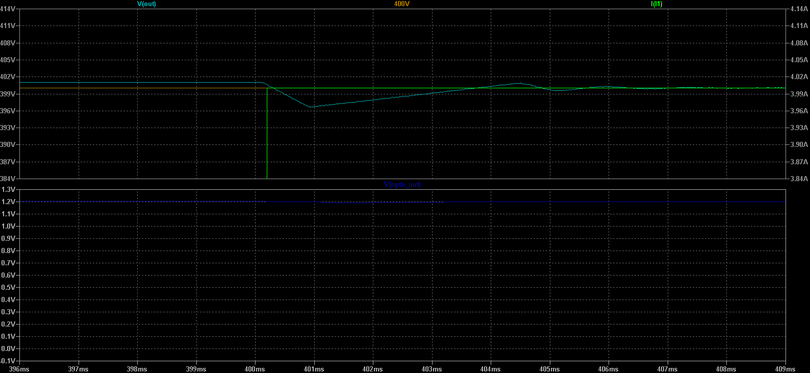
Figure 1: Voltage ramp-up / soft start. Load stepping after steady state is reachedFigure 2: Voltage transient / Stepping load from 0A to 4AFigure 3: Voltage transient / Stepping load from 4A to 0AFigure 4: MOSFET Drain current (spikes due to gate pulse and secondary diode recovery)
Model Information
LM317 model as well LTC3721 should be present in a recent Ltspice installation.
You may need Infineon’s IPP110N20N3 model.
This model has been tested on a Ltspice installation using the ZZZ (Ltspice groups.io community library), it is advised you install it.
For impatient visitors, the LTspice model download is at the bottom of this post.
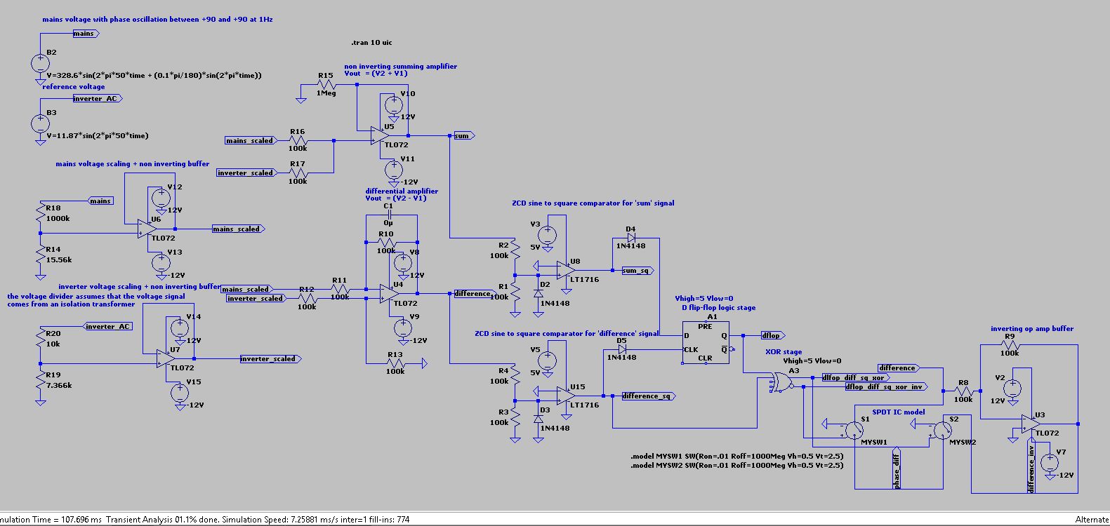
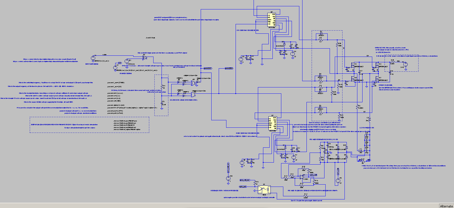
In our previous post we discussed the method that uses ZCD + flip-flops to extract the phase angle (angle of synchronism) using pulses whose duty cycle is proportional to the phase angle, and with a pulsing frequency of 2*f_ac, f_ac being the working frequency of the mains (grid) and inverter. Although this method is robust in the case of voltage variations, feeding pulses to our control loop required a more agressive low pass filtering strategy, and has a low gain at minimal phases angles, Overall it makes the control loop tuning harder.
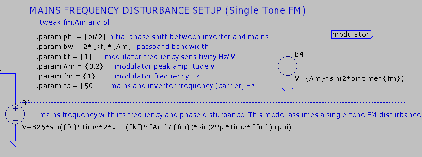
So we will propose now a time continuous analog estimation of phase angle. It closely resembles to the single multiplier phase detector in the shape of the output, but does not involve a multiplier. This method is projected to be significantly more sensitive to voltage swells/sags and transients or voltage imbalances between the mains and the inverter, as it is the case for most phase detectors used in PLL. So it will involve signal normalization as well. We will try to characterize the performance of this method compared to the classic mutiplier based phase detector. Same as in the previous post, here we are discussing of synchronized inverters, not grid tied ones. As such, these inverters, perform voltage control independently of the grid conditions, that is one of the main benefits of the double conversion (online) topology, that always supplies power coming from the inverter stage at a stable regulated voltage while the grid voltage may fluctuate. On the other hand, line interactive or offline UPS perform AVR only using an autotransformer with taps to buck or boost a voltage by fixed increments. Since we have a potentially fluctuating grid voltage due to external conditions and a UPS voltage regulated at a nominal value, (not taking into account voltage fluctuations due to regulation inertia), it is important to characterize the sensitivity to voltage imbalances of the following method to assess its viability for the purpose of inverter phase synchronization.
Principle of operation
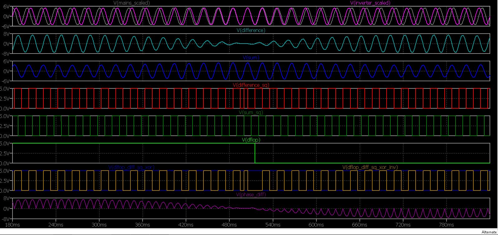
Instead of supplying the control loop a pulse whose duty cycle is proportional to the phase angle, with a postive pulse for positive phase angles and a negative pulse for negative phase angles. We supply the control loop the differential signal of V_mains(t) and V_inverter(t). That is V_mains(t) – V_inverter(t), after scaling the source signal to a level compatible with op-amps. Although it works to extract the absolute phase angle, assuming that the two voltages are of the same amplitude, preserving the lagging/leading information, that is the sign of the phase angle, requires careful processing of that signal.
Assuming a constant phase angle different than 0° and that the amplitudes of V_mains(t) and V_inverter(t) are the same,
We can see that the V_mains(t) – V_inverter(t) changes sign when V_mains(t) = V_inverter(t), although the lagging/leading status is still the same. That is why we need to switch the V_mains(t) – V_inverter(t) signal to -(V_mains(t) – V_inverter(t)) when V_mains(t) = V_inverter(t), to preserve lagging/leading information.
To encode the instant where V_mains(t) = V_inverter (t) using a basic sine to square circuit, we will feed the scaled down sum signal, (labeled ‘sum‘ in the schematic) V_mains(t) + V_inverter(t) to a comparator to get a square wave signal. The rising edge will happen at zero crossing going upwards of V_mains(t) + V_inverter(t), The falling edge at zero crossing going downwards. The points where V_mains(t) = V_inverter(t) will sit firmly at the middle of each HIGH or LOW levels time intervals. The resulting square wave signal is labeled ‘sum_sq’ in the LTspice model.
To establish a processing logic, We will also need to convert the difference signal, labeled ‘difference’ in the schematic into its corresponding square wave signal. This resulting signal is labeled ‘difference_sq‘ in the LTspice model. Note that the difference_sq signal switches polarity, that is, goes from RISE to FALL or vice versa at the points where V_mains(t) = V_inverter(t). More precisely, it is rising at V_mains(t) = V_inverter(t) when both V_mains(t) and V_inverter(t) are positive, and falling at V_mains(t) = V_inverter(t) when both V_mains(t) and V_inverter(t) are negative.
We used the LT1716 comparators for the ZCD sine to square conversion. It also conditions the square signals to 5V logic levels. It is tolerant to an input going down to -5V in relation to negative rail, here GND, while still outputing a valid 0V output in this case. This information is available in the datasheet.
Next we will establish a truth table for the above two signals.
TRUTH TABLE
difference_sq RISE
difference_sq FALL
sum_sq HIGH
1
0
sum_sq LOW
0
1
D flip-flop truth table
Note that we compare an edge signal to a level signal, for this edge triggered logic, a D type flip-flop comes handy. You may also ask why we need this convoluted logic, well it is necessary in order to preserve the leading/lagging information. In order to do that, we will need an additional logic stage between the above resulting signal, labeled ‘dflop‘ in the model, and the difference_sq signal. This time both signals are levels, so to establish the following truth table we will simply use a XOR gate.
TRUTH TABLE
difference_sq HIGH
difference_sq LOW
dflop HIGH
1
0
dflop LOW
0
1
XOR gate
The resulting signal will condition the state of the SPDT switch IC, the ADG333A IC is suitable for this application. The silicon SPDT switch will switch the output between $$ difference $$ and $$ \overline{difference} $$ input signals.
And that’s how we get an approximation of the phase angle, preserving the leading/lagging information. Note that the logic signal coming into the silicon SPDT switch not only has the result of switching polarity of the difference signal when the phase angle goes from leading to lagging and vice versa, but also performs rectification of the difference signal.
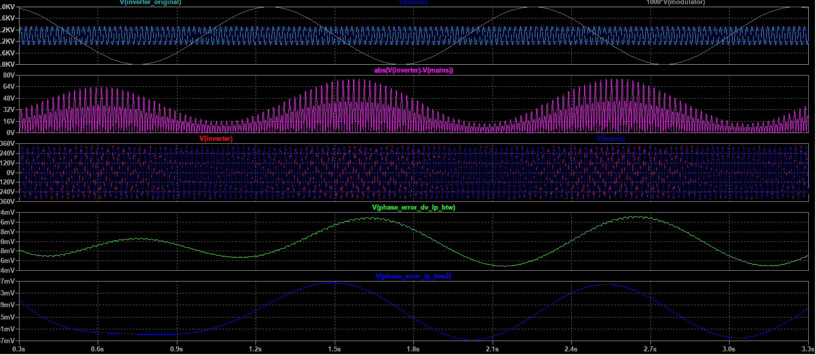
To better illustrate the action of the whole signal conditioning logic, we provide the following screen capture :
phase angle between inverter and mains oscillates between -90° and + 90° centered around 0°Logic of the continous phase angle approximation signal conditioning block
Now that we have our proper phase angle approximation signal, it is time to feed it to the control loop.
Remember from our previous post that, assuming same frequency and voltage for both signals, and a constant phase shift or a phase variation frequency that is negligible compared to f_ac :
Being sinusoidal in nature, it follows that for a time interval $$ (4)\hspace{1cm} \left [ t_{1} , t_{1} + \frac{1}{2f_{ac}} \right ] $$ or multiple thereof,
(3) is a linear relationship because $$ (5)\hspace{1cm} peak(k\times a(t)) = k\times peak(a(t)) $$ provided that (2) is true. Note that for the ZCD discrete phase angle method of our previous post, there is a linear relationship over the whole [ -pi , pi ] domain.
The main difference then lies into the LP stage filtering response of our control loop between a variable duty cycle bipolar square wave signal with 2*f_ac frequency and a bipolar sinusoidal signal with rectified sine harmonics at 2*f_ac frequency.
Phase angle control loop
We reused at first the phase control loop from our earlier post design :
Since this post, it has been updated with an additional integral term to get a PID control loop.
This loop already gave relatively good results (phase angle < 0.75° for most disturbances in our simulation bench). We used it too gather data in the new phase continuous model as a reference for improvement.
Then, we optimized the loop design to get a better phase response. For this, we got rid of the butterworth filters after the integral and derivative stages, as well as a tuning of the integral cutoff frequency and the derivative peak response frequency. We will post both results here as well as the Bode plot of the new control loop.
Voltage imbalance sensitivity
Voltage amplitude imbalance between mains_scaled and inverter_scaled has effects on the diff_out signal that are mostly characterized by a reduced sensitivity to small phase angles. The signal shows a larger DC bias, which swamps the response to angle variations.
The leading/lagging transition response seems less affected, the system being able to detect the transition in small phase angle oscillations, even in the presence of a moderate voltage imbalance.
Let’s discuss the possible mitigation strategies of the voltage imbalance sensitivity.
For the purpose of phase synchronization outlined above, the inputs of the control system are :
Inverter voltage sensing coming from an isolation transformer on the output of the inverter.
Mains/grid voltage sensing coming from another isolation transformer
Both of these inputs could also be used for voltage (amplitude) sensing. Inverter voltage sensing is already used for inverter voltage (feedback) regulation. If we wish to compensate the voltage imbalance for phase synchronization, we may need to sense both.
Voltage amplitude sensing methods usually implement peak detection using smoothing capacitors and a full bridge rectifier.
Inverter voltage is dictated by the inner voltage/current control loop and possibly an outer control loop. It is subject to a certain amount of inertia. Moreover, set/regulated voltage may well be different than the nominal 240V AC.
Mains/grid voltage is dictated by the grid. We also have to take into account the serial impendance of the transmission line and that of the 10kV/240V utility transformer. These will produce a voltage drop dependent on the load, and account for a large portion of voltage variation during the day.
If, for whatever reason we wish to implement the proposed method above we would need to get rid of the voltage amplitude difference.
Either we establish the mains voltage as a reference, and make the inverter follow it, by controlling the amplitude of the independently generated sine wave reference of the SPWM modulator. In that case, it defeats one of the main purpose of an inverter, specially for online (double-conversion) UPS, which is voltage stability independently of the grid.
We could also use the mains voltage as a reference to the full extent, after scaling it down, by using the mains voltage waveform as the sine wave reference used in the SPWM generation, in that case, the inverter also follows frequency and phase of the grid as a bonus, which render the whole synchronization issue of the present article moot. The downside is that the inverter output is now subject to all disturbances of the grid, including transients, noise, etc… if adequate filtering is not provided. The inverter now works as a class-D amplifier.
Third option, we establish inverter voltage as a reference, and make the mains (scaled down voltage input) follow the inverter voltage in terms of amplitude. Since we have no control on the voltage from the grid, the only method that seem plausible would be to perform AGC (automatic gain control) on the sensed mains voltage to make it follow the sensed inverter voltage.
The later is not without problems though. We predict that there may be quite a high amount of crossover interaction between the phase/frequency control loop and the voltage/current control loop, making tuning of both difficult. Let’s try nevertheless.
Implementing AGC on mains voltage sensing
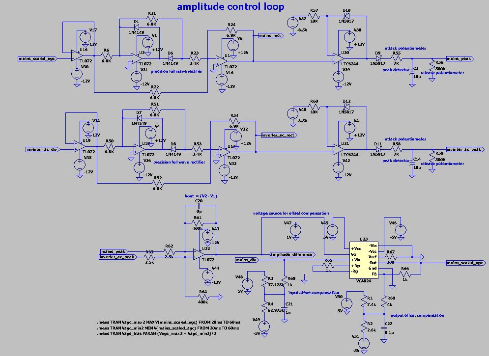
Since an inverter voltage control loop usually implements voltage sensing for its output using a peak detector (with attack/release control), And that doing the same for the mains voltage is also usually a requirement, for instance, to detect voltage sags/swell that go beyond the AVR capability, or simply for mains blackout detection, it seems that it would not cost much to at least try to implement an AGC for the goal of phase angle synchronization using the peak detectors outputs as differential inputs to generate a voltage control signal based on the voltage error that will be subsequently applied to a VCA. The VCA will perform AGC on the scaled mains voltage signal to keep it at the same amplitude that of the scaled inverter voltage. Then phase angle measurement can be performed without worry about the effect of amplitude imbalance.
The VCA would not need to have fancy requirements. It does not need high bandwidth, since it will work on a 50 Hz signal. It does not need high dynamic range, since it will operate on a mains voltage plus/minus 20% (worst case scenario) deviation from the nominal 240V AC. (Mains voltage is required in Europe to stay in the plus/minus 10% range from the nominal 240V AC.)
However, It would preferably use linear voltage control of the gain. That is to ease the loop design and tuning.
Voltage transient filtering (or what remains of it after the TVS upstream) could be achieved by tuning the attack potentiometer of the peak detector stage. However a compromise should be found between a good transient response and a good voltage following response so as not to introduce too much delay. This is not an easy task.
Given the requirements, a TI VCA824 IC seems a good choice. Other options although not tested would be to use an OTA like the LM13700, Finally we could also use an audio VCA like the THAT 2180x series, but it also OTA-like since it sources/sink current at the output, so either a resistor or better a current to voltage op-amp block is needed at the output. However the THAT 2180x is an exponential (dB/V) voltage controlled device, Whereas the VCA824 IC is linear (V/V). An advantage of the THAT 2180x is that it features a 0dB gain at 0V center point. It is not the case for the VCA824, Where the unity gain is closest to 0V gain control for a 2V/V max gain setup (dictated by the Rf/Rg feedback resistor setup). Even with a 2V/V gain setup the unity gain point is not exactly at 0V (at least in our setup). But this is not that much of a problem since there is a control loop for amplitude that takes care of it. Other issue encountered with the VCA824 IC is that we had to correct input and output offset voltages using voltage dividers at the signal input and output as shown in the datasheet. Using AC coupling for that purpose is a big no no since it would introduce delay. Finally, there is the cost issue. VCA824 is expensive and its features underutilized since it is tailored for HF/VHF use. But it works well for VLF like 50 Hz too. Finally, there is the issue of dynamic range. VCA824 can’t take much more than ± 1.6V at input, and goes sensibly lower than ± Vs for the output. Here Vs is ±5V (rail to rail) and this is the max for safe operation. To get some operational margin for voltage sags and swells, we setup max gain at 3V/V, and the whole setup works so as to obtain a normalized 1V amplitude mains signal, whatever the voltage sag/swell condition is. We expect the setup to be more sensitive to noise because of the reduced signal amplitude that is fed to the continuous phase angle measurement logic.
Amplitude control loop to get a normalized mains signal
Amplitude disturbance
For now, we only considered single tone FM disturbance of mains grid voltage. We still have to tackle amplitude disturbance like fast voltage transients with a clamped profile (from the TVS action), temporary overvoltages/undervoltages (from load rejection / load connection events in a generator setup), and slow voltage daily/hourly variations due to load profile change across several utility subscribers sharing a 11kV/230kV transformer.
First we will test the performance with a static voltage deviation from nominal 230V and see how the AGC performs, and how the whole loop behaves.
<to be continued>
Harmonics Disturbance
This is the hard part. It is expected that with a good voltage following characteristic, the whole loop would also somewhat track harmonics from the grid. Our goal would be to track the phase and frequency of the fundamental, not the harmonics ladden signal. We could think that filtering the mains signal would be a good idea, However we would need a really flat phase response (like those of Bessel filters), and even with that, we would need to compensate the delay with something like an all pass filter tuned to bring the 50Hz signal to a 360 phase or multiple thereof. That would introduce phase problems for frequencies other than 50Hz. Moreover, Bessel response is inadequate to filter the third harmonic sufficiently since it is so close to the fundamental. We could use a Butterworth LP filter but phase response issues would be even worse with each increasing order. We could think of a really good rejection of harmonics with a resonant filter, but that would be the absolute worse of the worse in terms of phase issues. Harmonics rejection is at the current state of analog filter technology an intractable issue in our opinion and would be better tackled in the Z-domain. Comment if you disagree.
Nevertheless, we added a harmonics disturbance setup in our model with 3rd,5th,7th,9th and 11th harmonics setup with amplitude (in % of fundamental amplitude) and phase (for each harmonic) to characterize the performance. At this point, the equation (3) is unsuitable, unless we compare the output sine reference to the fundamental of the harmonics disturbed signal.
Simulation Model
The simulation model includes the ASC Ltspice file with all packages dependencies (asy,sub,lib) in the same folder. There should be no need to tweak inside the file for absolute paths as they have been removed. No non-standard diodes, fet, bjt are used so there should be no need to add lines in the respective files (such as standard.dio or standard.bjt)
This model only models the PLL, not the full inverter. It’s goal is to generate a synchronized sine reference from mains voltage, and be tolerant to voltage sags/swells, frequency variation as well as harmonics. Harmonics should be rejected in the sine reference as much as possible.
Recently I added a block to simulate ADC operation with with sample time quantization and amplitude quantization to more accurately simulate an AD7366 ADC.
It includes a test bench block to simulate :
Amplitude disturbance
Frequency disturbance
Harmonics disturbance
Initial phase angle
It also includes the PLT files for plotting.
More information available in ____README____.txt inside the zip archive.
This is an introduction on inverter phase synchronization. The simulation files are included at the end of this post.
There are several digital and analog control methods to meet this goal.
In no particular order, we have DFT, KF, WLSE, ANF, KALMAN, PLL,FLL and ZCD. Most of them are documented in the digital (z-domain). A few only are easily implemented in analog.
We will discuss the easiest method, which is the zero crossing detection method, (ZCD) and assume that the inverter is not grid tied, simply synchronized.
Grid tie operation designs are diverse and fall into the grid following, grid forming, or grid supporting designs. This design is not intended for grid tie operation. These designs will be the object of another post.
The application goal, here, is mostly to have the inverter supply a voltage that is synchronized with the mains phase to enable seamless switching with an ATS that is external to the UPS, or inside the UPS unit independent of the technology used (offline,line-interactive or double conversion)
We will provide a hybrid analog/digital LTSpice model for phase synchronisation using the ZCD method.
It is “hybrid” in the sense that the inverter reference sine used in the modulation is phase modulated through a behavioural voltage source, that is more or less equal to what a DDS IC would do, but in a ideal manner since it comes without any quantization noise in LTSpice.
This model will be further updated. Note that phase synchronization using the ZCD method is performed using fully digital means in commercial ASICs. Providing a partially analog method is useful however for teaching analog control and for certain niche cases where the inverter SPWM generation and control feedback cannot be fully automated in the digital domain. (like using an Arduino instead of a fully capable DDS platform), In these cases, offloading part of the control loop to analog components is an option. Generally, fully analog control is less and less used except for simple feedback like in SMPS.
But there are still niche uses, for instance, an environment subject to ionizing radiation where hardening the ASIC is not possible, would be more robust in analog but that would require a fully analog control loop.
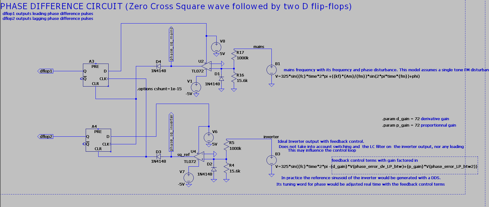
How to get phase difference between mains phase and inverter phase using ZCD the analog way ?
The analog ZCD method translates a sine wave (here, the output of the inverter or that of the mains power) into a square wave signal. the rising edge of the square wave signal happens at the upward zero crossing of the phase, and the falling edge at the downward crossing of the phase.
ZC sine to square wave conversion is done both for the mains and inverter phases. This is done using an op-amp comparator without feedback for each phase. The output signal is a square wave with rail to rail voltage levels.
Then, the two square signals are compared using two D type flip-flops, giving outputs pulses widths that are equal to the absolute phase difference information. (it outputs time information, not an angle value)
The method is explained in “Phase measuring circuit with leadlag indication” by Forrest P. Clay Jr. a 1992 electrical engineering paper.
This method preserves the phase lag/lead information. One flip-flop provides HIGH output in leading conditions, While the other provides HIGH output in lagging conditions. Fundamental pulse frequency is the same as the mains and inverter frequency (assuming that both have a frequency deviation that is negligible compared to the nominal frequency) that is, 50 Hz in the model.
Phase difference detector circuit used in the simulation
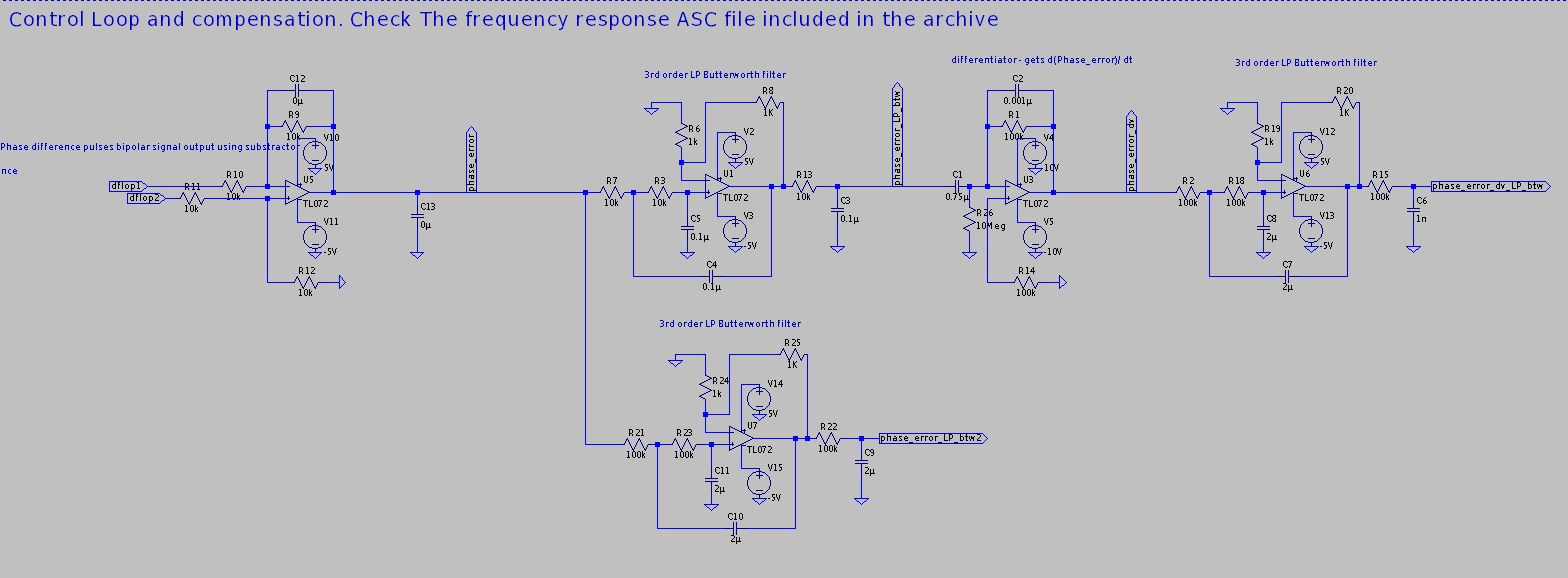
Then, the output from the flip-flops is given to an op-amp substractor that generates a bipolar signal of the phase difference. Positive pulses mean leading while negative pulses mean lagging. Care must be given to the resistors tolerances (1% or better) in a substractor to minimize common mode interference, and a suitable OpAmp for this kind of use is prefered.
This signal is then low pass filtered to remove edge induced discontinuities. Note that usually the mains frequency slew rate is really slow because of the huge rotational inertia of all generators creating the mains distribution network and all regulation mechanisms in place. So it is not a problem to have a filter with a very low cutoff frequency. On the other hand, if the inverter were to synchronize to an islanded generator, that would be a whole different scenario. It is outside the scope of the current article. For these scenarios, other synchronization methods exists, and we named a few at the beginning of the article.
The filter used is an analog 3rd order butterworth LP filter, to get a sharp rolloff. The first stage has a quite high corner frequency, in order to minimize filter phase effects at low frequencies. Its goal is to minimize rising and falling edges coming from the ZCD and flip-flops well enough for the differentiator stage not to complain.
We then get a smoothed phase shift signal $$ \Delta \varphi $$ . This is fed to a differentiator op-amp setup. Its role is to generate the $$ \frac{d(\Delta \varphi )}{dt} $$ signal used further in the control loop. Note that because of processing this signal has a delay, so our notation is a little it abusive.
This signal is further processed using a second 3rd order butterworth LP filter, with a corner frequency way lower than the first butterworth filter. This gets rid of the spikes in the signal. The corner frequency is around 1Hz.
This concludes the generation of the $$ \frac{d(\Delta \varphi )}{dt} $$ processed signal that will be fed to the control loop of the inverter, for the derivative term.
In parallel, we need to get the proportional term. This will use a single butterworth 3rd order LP filter that branches just after the substractor. This will generate the proportional term also fed to the control loop of the inverter. This filter has a lower corner frequency compared to the first LP filter stage used for the differentiator branch.
Note that the final butterworth filter of the derivative signal branch has been slightly tuned out from its canonical form to get an appropriate control loop frequency/phase response.
Other than that, the remaining filters are quite the same. The differentiator has an added C2 capacitor to filter high frequency terms and provide less oscillation.
These two signals (proportional and derivative) are then factored with their respective gains (both are the same in the simulation) and fed as a sum to the behavioural voltage source of the inverter using the phase term of its function.
Note that this is a simplified model of the inverter stage. A more realistic but computationally intensive model would control the sinusoidal reference of the SPWM stage of the inverter, and inverter output would be fed to one leg of the phase difference detector. This would integrate the whole SPWM inverter model to this simulation. Note that this simulation do not include RLC loading of any of the phases. Also, this model supposes that the mains and inverter AC voltages are the same and stable at AC RMS = 230V.
One advantage is that the ZCD method is quite tolerant to voltage variations, compared to methods that are sensitive to it like PLL, So It is not critical to have it factored in this simulation.
Control loop. Not shown the final mixing stage that happens in the BV sine source of the inverter
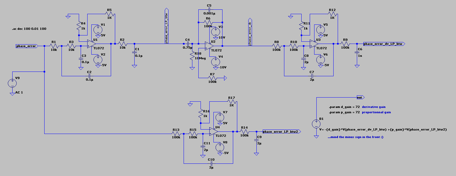
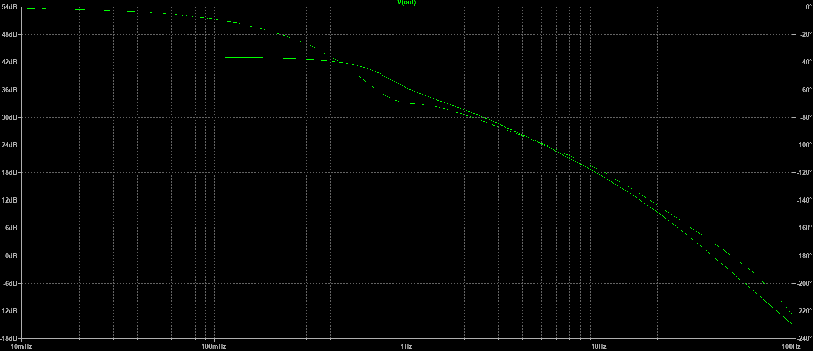
AC Analysis of the control loop
An open loop AC analysis starting from the input to the first LP butterworth filter up to the output of the sum of the derivative and proportional terms with their respective gains has been performed.
Content of the control loop AC simulation fileBode plot of the control loop. Plain line is Gain, Dotted line is phase
The range of frequency analysis for our first inspection is 0.001 Hz to 100 Hz
The cutoff frequency is approximately 0.66 Hz
The DC Gain is approximately 43.2 dB with a flat response.
Gain margin is -3.5 dB (at f_GM = 48.1 Hz) This could be improved for stability, knowing that this frequency is quite critical being close to the 50 Hz component in the phase difference pulse signal.
Phase Margin is 9.8° degrees (at f_PM = 38.6 Hz). Phase margin could also be boosted. Phase margin stays positive below f_pm.
There is a pole around 0.66 Hz and another close to 1 Hz, barely visible in the plot.
The control loop will be further optimized when I have time. I am no guru of control loops and filters so if you manage to get an optimized model, please chime in using the contact form…
Mains Disturbance simulation
Frequency disturbance
The first goal is to characterize how tightly the inverters locks on the mains frequency that is, $$ min(\Delta \varphi) $$ and $$ max(\Delta \varphi) $$ for a given mains frequency disturbance scenario. We also used a simple function to get an idea of the magnitude of the absolute phase difference by plotting $$ \left | V_{inverter} – V_{mains} \right | $$ and look at the local maxima. note that this plot does not suffer from the delays coming from the LP filters.
Simple FM disturbance
The disturbance scenario modeled this far is a mains frequency oscillation with a parametrized slew rate and oscillation amplitude, using a simple FM modulation scheme. The peak instantaneous frequency deviation will be restricted first to ±0.2 Hz to get in line with the ENTSOE ordinary and contigency frequency deviations, that is, an oscillation between 49.8 and 50.2 Hz
Frequency Stability Evaluation Criteria for the Synchronous Zone of Continental Europe
Since time keeping by these clocks rely on the number of cycles of the mains period, it makes sense to calculate the phase error. This study precisely do this, measuring phase deviations and not only frequency deviations. Phase errors in a power distribution grid come from frequency instability. To compensate for phase errors, an utility company would have to precisely manage frequency compensation at regular intervals to “get back” to the theoretical number of cycles expected. The priority is frequency, not phase, and mains tied clocks are superseded by GPS. However, this anecdotal study is however of special interest since we are dealing with both frequency and phase adjustments in grid synchronization. Note also that an abrupt phase adjustment in a rotational generator such as synchronous machines used in power plants would come from disastrous events such as pole slipping and/or sudden uncompensated load rejection. It should never happen on the scale of an utility grid.
As for the frequency, the slew rate for mains frequency is extremely low in ordinary and even contingency modes, So a rate of 1 Hz is already an extreme worst case scenario. Higher slew rates however happen with islanded generators, but this is outside the goal of this simulation. Given the response of the control loop, low slew rates should not pose a stability problem. However, this depends on the detection threshold of the flip-flop stage. A minimal instantaneous frequency deviation would not be catched until it reaches this threshold.
Note also that frequency deviations include stochastic noise but also predictable deviations according to load consumption and power generation imbalances. Periods of high demand typically introduces a negative frequency deviation until the power generated matches the load power.
As said before, the ZCD method is sensitive to harmonic disturbances typically introduced in non-inverter type islanded generators with low power handling capability relative to load. Thus, further characterizing the control loop for worst case scenarios would need to introduce this kind of disturbance, if one were to use ZCD with generators nonetheless.
Amplitude disturbance
<to_be_continued>
Phase synchronization from arbitrary initial phase difference
The other goal of the simulation is obviously to track the performance of phase locking from an initial arbitrary phase difference. The inverter has to lock its phase at 0° degrees phase difference from any starting phase difference ranging from -180° to +180° degrees. The performance of this locking process, that is how fast the phases converge to 0° and if the inverter experiences excessive harmonic disturbances during this process will have to be characterized.
Assuming both mains and inverter voltages are of the same amplitude, perfectly sinusoidal, and that the inverters track frequency change instantly or that the simulation is performed at fixed AC mains frequency, performance of phase synchronism can be measured through the following formula, giving the the absolute value of voltage phase difference.
Since the ‘periodicity’ (the periodicity of the mains frequency induced harmonic component) of the function above is $$ \frac{1}{2f_{mains}} $$, that gives the optimal sample time to extract the maxima when sampling the above function (1)
The above function (1) can be simply plotted. If you need to extract maxima at sampled intervals use these LTspice directives and loop them with subsequent time intervals of $$ \frac{1}{2f_{mains}} $$ and put them into a .MEAS file, although it would need a long simulation time to make sense. For complex data analysis it is better to make a LTspice export of the data and process it with Python for instance.
.meas TRAN Vdiff_abs_norm_max MAX (abs((V(vl) -V(vn)) - V(mains))/(2*1.414*{V_ac}) ) FROM 0ms TO 10ms
.meas TRAN delta_phi_abs_max PARAM 2*asin(Vdiff_abs_norm_max)
measuring the minimum phase difference (best performance at steady state) is less trivial because of zeros in the function when the sine waveforms cross each other, therefore it would require sampling the phase difference with the above method and then analyze the resulting data for local minimums. Overall, another useful metric is simply done by averaging the sampled maximum phase difference (CTRL+click) for function (1) over a long interval, preferably equal to a full oscillatory cycle that arises from the control loop, if one is found.
Finally, performance in phase locking has to be demonstrated in conjunction with a FM disturbed mains frequency.
Note that phase locking is preferably done while keeping the waveform sinusoidal in nature during the process. Phase locking in figure 2 happens too quickly, and has the effect of producing severe distortion. The inverter should have adequate protection to not supply power during this event, only after proper phase locking is done. In a mains synchronized double conversion UPS, this could happen if the input is switched between two phases (120°shift) or after the powering on and transfer to a generator. Since a double conversion UPS always provides power through the Inverter stage with no possible downtime except a minimal one for switching to and from bypass mode, the control loop has to be tuned to take that into account. A modification of the phase control term in the sine wave DDS generator could be done and would take effect only during these initialization/switching events, for instance, using
$$ 1-\exp\left(-a\cdot t\right) $$
as a factor of the control term, ‘a’ controlling how fast the control loop locks into the mains phase.
Simulation results
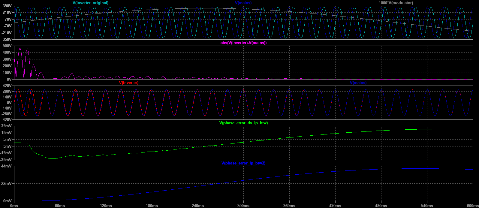
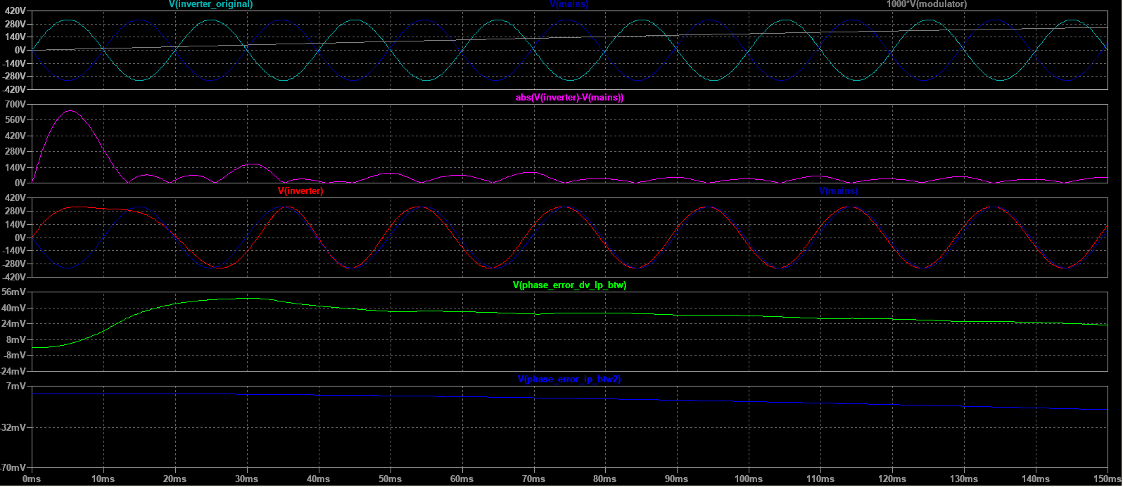
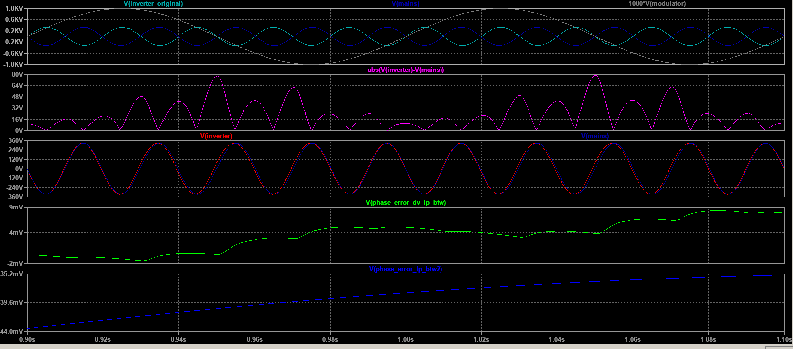
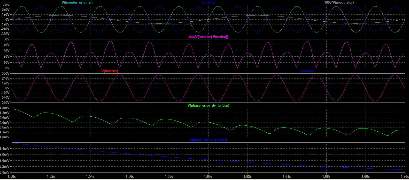
Fig. 1 initial phase difference +90° , frequency disturbance : modulator freq. fm = 1Hz, modulator Amplitude Am = 0.3VFig. 2 Initial phase difference +180°, fm disturbance unchanged. Note the large disturbance of inverter phase during the lock process. Locking happens in less than a periodFig. 3 frequency disturbance : modulator freq. fm = 1Hz, modulator Amplitude Am = 1VFig. 4 frequency disturbance : modulator freq. fm = 1Hz, modulator Amplitude Am = 1V At this slew rate of mains frequency and high frequency deviation, performance is degraded.Fig. 5 frequency disturbance : modulator freq. fm = 1Hz, modulator Amplitude Am = 0.3
Using the ZCD method, sampling time is limited at two times the mains AC frequency. That limits accuracy of the algorithm for fast and ample disturbances. But a heavily distorted power source would not lead to any application requiring syncing into it, rendering that issue moot.
On the other hand, ZCD is quite tolerant to voltage fluctuations.
Conclusion
Although this controller is simple to implement, it suffers from steady state error due to the limited gain at DC. One option to mitigate this is to add an integral component. However, it would still suffer from delayed response to oscillations due to the butterworth filters, and cannot track fast oscillations. The ZCD+Flip Flop stage also samples phase at 1/2*f_ac, which is a limiting factor. The non linear behaviour introduced by the discrete function of the flip flops, who encode phase difference as a pulse further make the tuning of the control loop harder, with the need to analyze the impulse response of the system. However the discrete ZCD phase difference method is more robust when it comes to voltage imbalance between the two measured phases.
In a next post, we will propose a time continuous control of phase difference without flip-flops in the control loop signal path (although one is still needed in the circuit).
To get back to the conclusion on this model : Its performance level is unacceptable for grid tie operations, nor it provides the required functions and behaviour of GFL,GFM,GS grid tie topologies. That is why we limit it to synchronization for inverter standby/autonomous operation to alleviate source switching transients. But it is a good introduction on the subject. For an idea, it is closer to the state of the art for the start of the 90s or so, when digital control was not yet so widespread.
We will discuss grid tie inverters in a later post and slowly but surely move into the more state of the art technologies. It will also serve as an introduction into fully closed loop control systems, as with grid tie inverters, voltage,current quantities are intimately tied, and reactive power effects have to be taken into account.
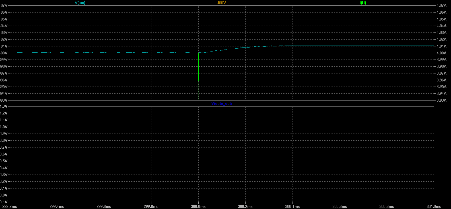
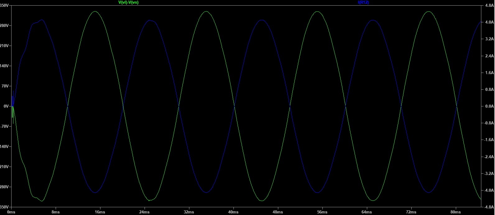
output voltage and current waveform, 80 ohms resistive load
Disclaimer : This design uses dangerous AC and DC voltages. If you get out of the simulation domain and start prototyping be sure to use all safety precautions required when working with high voltages. You have to know what you are doing.

Besides the simulation this post is an introduction on pure sine inverter technology targeted at electronics engineers that have little or moderate experience in power electronics and inverter design.

The goal is to design, implement and prototype your own pure sine wave inverter from scratch as an educational project to get into inverter technology, this will be the object of a series of posts in the future.

For a faster design approach see the bottom of this post on how to use off the shelf inverter modules such as EGS002 or EGS005 available on BangGood and AliExpress.

To get straight into the model simulation go to the running the simulation section.

Introduction

Inverters use MOSFETS to switch a DC source with a variable duty cycle PWM signal.

The duty cycle variation in the time domain is performed at the frequency of the required output fundamental frequency of the inverter.
Usually mains frequency, that is 50hz or 60hz.

The frequency of switching, that is the frequency of the PWM signal is called the switching frequency. it is usually in the 2.5khz to 100khz range.

So, the goal is to have a PWM signal at high frequency (2.5 khz to 100khz) with a variable duty cycle whose frequency is at mains frequency.

However, The variable duty cycle frequency may be lower or higher, or can be adjusted in real time.

Applications that require this duty cycle modulation at fixed but non standard 50Hz or 60hz are mainly for the aerospatial industry.

Airplanes use 400hz. The advantage of 400hz is that power transformers are less bulky than in 50Hz.

There is also an industry need to adjust the inverter output frequency in real time. This is the market segment of VFDs (Variable Frequency Drive) inverters.

This allows to set the rotation speed of induction motors, and allow for a soft-start that does not damage the motor.

In VFD applications, not only the the frequency output of the inverter is managed, but also the output voltage, and sometimes they implement a fixed voltage to frequency ratio mode so the motor stays happy.

So, now comes the question, How to modulate the duty cycle of a PWM signal ?

This is usually done by comparing a triangle signal at the switching frequency with a reference sinusoidal signal at the desired mains frequency.

This can be done in two ways :

1) Using analog components : a sine generator IC (like the XR-2206 or MAX038) that outputs a triangle wave and another one (also XR-2206 or MAX038) that outputs the sine wave. Then, a schmitt trigger is used to compare these two signals to output a PWM signal.

2) Using digital components : the sine modulated variable duty cycle PWM output is generated by code running on MCUs, PIC, DDS IC. Arduino can do this, however Arduino has a limitation that hinders its use for this purpose, and that is dead time control. More on this later.

If you nonetheless want to experiment with SPWM generation with an Arduino, check this code to get an idea of how it works.

I recommend you read resources on Fast PWM for Arduino. It is not straightforward if you have no experience with hardware counters/timers. Check https://www.arxterra.com/tutorial-on-fast-pulse-width-modulation/ and https://docs.arduino.cc/tutorials/generic/secrets-of-arduino-pwm
for starters. You may have to browser for other resources because I could not find one comprehensive documentation for ALL modes, except maybe in AtMel datasheets, but these are very terse and quite hard to understand.

Here is the first code sample :
#include <Arduino.h>

uint16_t freq = 50; // inverter output frequency
uint32_t counter = 0;
uint16_t mod_index = 0.9; // modulation index. you will have to update this in real time for precise voltage control.
float sin_val;
const uint16_t samples_per_period = 100;
// higher samples per period give a better looking output sine wave, less harmonics from digital aliasing
uint16_t micros_interval;

uint16_t sin_table[samples_per_period];

void populate_sin_table()
{

  uint16_t i;
  for(i=0;i<samples_per_period;i++)
  {
      sin_val = 512*(1 + mod_index*sin(2*PI*float(i)/samples_per_period));
      sin_table[i] = round(sin_val);
      //Serial.println(int(sin_val));
  }

}

// FAST PWM PHASE-CORRECT MODE 3

void setup(){

  // Wave Form Generator: phase correct PWM mode 3, Top = OCR1A and OCR1B
  // We will output two signals, complementary, using two pins ~9 and ~10 so we need to specify
  // (0<<COM1A0) + (1<<COM1A1) + (1<<COM1B0) + (1<<COM1B1)
  // (0<<CS10) + (1<<CS11) + (0<<CS12) this is the prescaler and will dictate the switching frequency.
  // (1<<WGM11) + (1<<WGM10); and (0<<WGM13) + (0<<WGM12) are used to set the Fast PWM mode, here we use mode 3.
  // it allows a 10 bit amplitude resolution for the sine wave signal
  // check this link for a table of available modes.


  TCCR1A = (0<<COM1A0) + (1<<COM1A1) + (1<<COM1B0) + (1<<COM1B1) + (1<<WGM11) + (1<<WGM10);
  TCCR1B = (0<<WGM13) + (0<<WGM12) + (0<<CS10) + (1<<CS11) + (0<<CS12);

  OCR1A = 0x3FF; // top compare value initialization. it will be varied using the sine table in the loop.
  OCR1B = 0x3FF; // same for the second PWM signal

  //DDRB |= (1<<PB1);

  //Serial.begin(9600);
  populate_sin_table(); // create a sine table. better use PGM write and store it in flash for a more robust approach
  micros_interval = int(float(1E6)/(float(freq)*float(samples_per_period))); // the loop wait delay between two bit bangings
  // of OCR1A and OCR1B.

  //Serial.println(micros_interval);

}


void loop() {
 delayMicroseconds(micros_interval);
 OCR1A =  sin_table[counter%samples_per_period]; // iterate on the sine table, use modulo to loop the table
 OCR1B =  sin_table[counter%samples_per_period]; // same for the second SPWM

 //Serial.println(sin_table[counter%samples_per_period]);
 //Serial.flush();
 counter++; // overflow not managed !!!!!
}
There is also this wonderful code https://forum.arduino.cc/t/dead-time-between-pwm-signals/937405 for a three phase system. I did not test it but it looks serious and legit. It has the advantage of using ISR and not a loop to update the TOP value with the sine wave, generates 6 signals (so it is for bipolar spwm) but it suffers from the same dead time insertion problem however, and that is the object of the guy’s post. But it is possible with analog post processing, check the DTI section.
That is why STM32 based boards are better for an all digital SPWM generation purpose, but they are more expensive and you'll need to watch quite a bunch of tutorials to master Nucleo (the STMicroelectronics MCU IDE). It will be easier if you already master Arduino FastPWM generation, but it will require time nevertheless.
Now is a good time to learn about the specifics on how that sine modulated variable duty cycle PWM signal allows the inverter to generate a 50hz, 60hz or higher frequency mains power phase voltage.
The "sine modulated variable duty cycle PWM signal" will be now referred by its usual name in the power electronics technology as SPWM (sine PWM)
The power core : the MOSFET H-bridge
The power core of an inverter uses an H-bridge configuration because the setup of its components ressembles to the letter H.
It is one of the most common designs in the industry.
MOSFETs switch repeateadly a DC source with low source impedance (the power source) according to the input gate signal that comes from the SPWM.
That is not all. high VDS high current MOSFETS usually need gate voltages that are higher than what an MCU or an analog oscillator can generate.
The high side MOSFET gates of the H-bridge also need voltages with reference to DC ground that are way above the levels of the logic/analog controllers.
For that reason, there is a specific family of ICs that exists and they are called "MOSFET Gate Drivers". Their goal is to bridge the gap between the logic SPWM signals and the required voltage levels (and current requirements) of the MOSFET gates.
Moreover, an H-bridge inverter has at least 4 mosfets. These MOSFETS need to be activated by gate signals at a precise fashion, like a fine tuned choregraphy.
The activation pattern is usually diagonal in the schematics. This has the effect of reversing the polarity with reference to DC GND seen by the load with each pwm pulse. Since the two SPWM signals are complementary in this design, when one diagonal set of MOSFETs has a high duty cycle it will be on and conduct a longer time than the reciprocal diagonal set of MOSFET, when this happens the output sine wave of the inverter is at a +Vo_peak. Then there is a time when the duty cycle 0.5 for both diagonal pairs, at this point the sinusoidal output of the inverter crosses 0V. then the cycle goes in the reverse direction and outout reaches -Vo_peak.
PWM Modulation schemes
I just described one SPWM modulation scheme. There are two schemes that are most commonly used.
- Unipolar SPWM
- Bipolar SPWM
To understand the difference between the two, please read now :
https://www.sciencedirect.com/topics/engineering/sinusoidal-pulse-width-modulationhttps://www.tntech.edu/engineering/pdf/cesr/ojo/asuri/Chapter2.pdf
My guide is based on Bipolar SPWM.
As you may already guessed, for that SPWM scheme you need two complementary SPWM signals.
For analog SPWM generation, the original SPWM signal generated from the triangle to sine comparator is fed to a NOT gate to create a complementary SPWM signal.
The original signal will drive the Top Left MOSFET and Bottom Right MOSFET
While the complementary signal will drive the Top Right MSOFET and Bottom Left MOSFET.
Note that in an unipolar SPWM scheme, The complementary SPWM signal stays low the whole time the other one operates, and then starts doing SPWM modulation while the other one stays quiet. This switching happens at 2*f_mains,
I find it harder to generate these two kinds of SPWM signals using digital means, so I think that the bipolar scheme is better to start grasping the technology.
Note also that IC Gate Drivers usually manage two MOSFET for a half bridge configuration. So we need Two gate driver ICs
In the LTSpice model IR2110 is used, as it is quite common in the industry.
The routing between the SPWM signals and gate drivers is as follows in my LTSPICE schematic and simulation :
SPWM signal is provided to HIN input of Gate Driver 1 and LIN of gate Driver 2
Whereas the complementary SPWM signal is provided to LIN input of gate driver 1 and HIN input of gate driver 2
HO output of gate driver 1 drives the top left M1 Mosfet
LO output of gate driver 1 drives the bottom left M2 Mosfet
HO output of gate driver 2 driver the top right M4 Mosfet
LO output of gate driver 2 drives the bottom right M3 Mosfet.
If you connect the dots, you'll see it fits the requirements of bipolar SPWM modulation scheme.
The big issue : dead time control.
There is a factor that needs extra precautions because it can fry the MOSFETs and brick the inverter. In no case, the M1 M2 MOSFETs should conduct at the same time.
This also true for M4 M3. If that would happen, The low impedance DC source will short through these MOSFETs (from Vdc to GND). When driven to high gate voltages, these Power MOSFETs have a ridiculously low RdsOn, This will generate currents way above the absolute ratings of the MOSFET, frying them if a DC breaker or another protection from the upstream DC link did not catch it in time.
For this reason, a security margin between the two SPWM signals (the original and complementary) has to be put in place, This is a delay between pulses where both SPWM signals remain low. This is called dead time.
a good article to read on that subject :
https://hackaday.io/project/3176-gator-quad/log/11741-pwm-control-and-dead-time-insertion
For digital SPWM generation, forget about Arduino to get SPWM plus dead time control using Phase correct PWM out of the box.
Better PICs or MCUs are required such as STM32.
It is however possible to apply analog treatment to a single SPWM arduino generated signal, to create a complementary signal with a dead time delay inserted before the rising edge and after the falling edge.
In the supplied schematic, it is done through a RC network whose time constant is matched to introduce the required dead time, plus a bunch of gates and schmitt triggers. This setup may be simplified, if you manage to use less components or update the model to use real world components instead of ideal ones, let me know through the contact form.
Output Voltage controland regulation.
Output voltage control of the power stage is performed basically by varying the triangle peak voltage, while the sine voltage remains the same.
The peak output voltage is roughly given by
Vo_peak = V(dc)*V(sine)/V(tri)
Vo_RMS is then V(dc)*(V(sine)/V(tri))/sqrt(2)
V(sine)/V(tri) is known as the modulation index (mi)
it is usually < 1
If V(sine) gets larger than V(tri), the inverter operates in the overmodulating region, and RMS output voltage is no longer linearly dependent on V(dc)
It appears in the simulation as a voltage saturation of the output.
overmodulation is outside the scope of this guide but it is explained in the above mentioned resources.
An open loop control is not realistic because of deviations from theory that assumes ideal components, and dependance on the load RLC parameters and the output filter parameters, as well of the transformer if an isolated output is required.
So there is a need for a voltage feedback loop to the SPWM generating component to adjust the modulation index.
Passing the voltage information to the source controller has to be done properly.
Because of voltage shifts of the (V(l) - V(n)) voltage relative to DC GND even after passing a voltage divider in this unisolated design, galvanic isolation is required, and this is a safety requirement.
If the output is isolated using a mains frequency transformer, galvanic isolation in the feedback loop is inevitable.
There are three methods to create an insulated voltage feedback loop.
- Using an auxilliary winding in the secondary of a mains transformer.
With a turns ratio tuned for low output voltages, usually such as 3.3V/2 (rms) or 5V/2 (rms) is obtained when the inverter output voltage is at nominal conditions. That gives ample room for the signal to go higher if the output stage encounters an overvoltage situation.
One leg would be connected to DC GND, the other fed to a full bridge rectifier, smoothed, and then that voltage would be fed to an error amplifier op-amp (a difference amplifier) that compares it to a precise voltage reference. This difference signal is a negative feedback that is then used to adjust the modulation index if using full analog generation. That would happen by controlling the AM pin of the XR-2206 Triangle generator, for instance.
If the SPWM is generated with digital means, the error amplifier could not even be required.
A DAC may be enough to acquire the voltage output of the optocoupler and the comparison of the DAC output would be done against a digital reference. Then, a digital control method should be implemented to control the feedback loop (such as PID) and update the modulation index.
I digress. Back to the feedback isolation.
- The other way of isolation is to use a separate low power transformer, with it's primary legs in parallel with the load. That is useful if your design does not use a transformer at all for the power stage, so you need only a transformer for feedback. Also, transformers with auxiliary windings are specific and you may have one on hand without that feature.
Of course it should be designed for 50Hz, or 60Hz, or more depending on your output frequency, with a ratio adjusted the same way as for an auxiliary winding.
- The third method involves a rectifier, a smoothing capacitor/filter stage, a voltage divider, which output drives a voltage controlled current source.
In this design I am trying a modified Howland current pump.
This current source is required because it will drive an optocoupler to transmit the analog information across the insulation barrier.
Optocouplers are current driven.
Care has to be taken to operate the optocoupler in its region where the CTR (current transfer ratio) is linear, by setting properly the current source gain.
Then one has to chose the proper collector resistor on the output side of the optocoupler to obtain proper transfer characteristics.
It is advised to test the transfer characteristics of the Current source + Optocoupler in a separate circuit to tune it up before adding it to the design, it will make things faster to simulate and way easier.
The rest of signal processing is the same as with the transformer approach.
Either digital control if SPWM is generated through a MCU or analog if using an oscillator. Analog will need a compensation network (usually a R+C // C) network for the feedback control loop to be stable.
Note : I have yet to model this part in the supplied model. It will be the object of this post revision in the future.
However, the fact that we are dealing with an inverter and that we have to perform rectification and smoothing to extract the peak voltage information, introduces feedback charateristics that are a bit different than DC/DC converter feedback loops.
Since the feedback loop would be designed with non-monolithic components (By that I mean the that the feedback loop does not use complex IC whose internals are a black box if their full transfer characteristics are not provided in the datasheet, and that perform mysteriously during AC analysis), it is possible to perform an AC open loop frequency response analysis of the rectifier + smoothing capacitor + current source + optocoupler quite easily.
Then add and tune a proper compensation network to obtain stability.
Check this guide for an introduction on compensation networks. It is targeted for SMPS power supplies, but the core concepts are the same, that is the need to model the open feedback loop at steady state, introduce a perturbation, and perform an AC analysis to get the frequency and phase response. (The bode plot)
https://www.ti.com/seclit/ml/slup340/slup340.pdfThe LC output filter.
A LC filter is a second order passive filter.
It's goal is to filter the high frequency switching pulses to obtain a pure sine wave with the least amount of harmonics.
In that design, I set the fc (corner frequency) at 10 times the mains frequency, that is 500Hz, not that the lower this frequency, the larger the L and C values, and the larger the effects on voltage with changing load impedannce.
You will notice also that the sine waveform THD will change with loading, appearing less distorted at higher loads
Finally, the LC output stage has an effect on output power factor. An inverter designed for inductive loads will be tuned differently in that regard.
Loading of the filter also affects its response and hence change the output voltage.
Check this thread for a discussion on inverter LC filters :
https://www.edaboard.com/threads/true-sinewave-inverter-output-lc-filter-design-help-needed.375327/Running the simulation.
Download the zip file in the post introduction. Check the readme.txt in the zip for important information about LTspice setup for that model. Most of the important parameters are parametrized and explained
Most of the inverter functional blocks have commentaries that complement the information given here.
On a core i5 Elitebook 8440p, using LTspice under Wine on Linux, I get around 6.5us/s simulation speed. Try to get at least two or three output sine periods.
This is a work in progress, it will be updated as I improve the model.
A faster approach.
Fortunately, you don't have to reinvent the wheel if you have no time to learn all the intricacies of inverter technology, It is however always better to have an understanding of how all the inverter components work before using a board that implements some of the inverter functions in their design.
For this, there are inverter boards, and we'll have to turn to China and EGMICRO
EGMICRO is a supplier of ASIC inverter boards and more that take care of the SPWM thing, DTI, Gate driving, frequency settings, and voltage feedback, plus they have a monitoring output. They can be used for UPS inverters and also for VFD operation. They also have 3 phase boards.
For single phase designs, there are three ASIC demo boards sold on the market :
- EGS002 is an older but still popular demo board that features the EG8010 ASIC and two IR2110S gate drivers.
I used the same gate drivers in my LTSpice model.
- EGS005 is an newer demo board that features the EG8025 ASIC. It is a monolithic design with integrated gate drivers.
- EGS003 is a board available on the market, with a EG8011 ASIC, plus a single EG2126 package housing a full bridge Gate Driver. But It was since discontinued (the EGMicro website purged the documentation about EG8011) It may have been superseded by EGS005 or it may suffering from issues. Suppliers still sell it. The EG8011 ASIC datasheet still can be found elsewhere. I do not recommend that design if the ASIC supplier made it obsolete.
We will nevertheless perform some intel gathering on these three designs to see how they differ in their reported features.
For three phase designs, There is an EGSO31 board based on the EG8030 ASIC. It uses separate EG3012 gate drivers instead of the more ubiquitous IR2110. A three phase design is necessary for VFD designs powering 3 phase induction AC motors.
To get and idea of how these devices work, you need to check the Demo board, the ASIC and the Gate driver datasheet.
Some of the PDFs are available in simplified Chinese only, but you can pass it to Google translate and have a quite precise idea of what does what after sometimes a little guessing. The quality of Google's technical translations is quite good, since these are terse statements and not litterary works.
The goal is to look precisely at the application schematic and adapt it for our needs.
We will start by investigating the EGS002.
Check that GreatScott's video on EGS002 as an introduction, it also uses a demo UPS board (not just the ASIC+driver board)
https://www.youtube.com/watch?v=Dn2PFebi2ww
Please keep tuned for part II. Where we will discuss EGS002 in more detail to unveil its secrets.
The inverter stage of UPS or Grid tie inverter technology
The rectifier and PFC stage of PSUs
And make use of a renewable power source such as solar panel array
The core of the design is a DC/DC converter with MPPT, current sharing, battery management, It uses an auxiliary AC power input to allow for operation when solar panels do not provide enough power.
Such designs already exist, but they usually contain an inverter stage to output pure sine mains voltage AC.
The hard part of these designs, whether they contain an inverter stage or not at the output is the current sharing stage. Finely controlled current sharing requires voltage control of all the input sources. However, the output DC/DC step up/down converter stage that conditions solar panel output is dictated by the MPPT algorithm. The solution then is to perform control of the voltage output of the mains AC/DC step up converter stage.
However, by doing so, the load impedance seen by the solar DC converter changes, and upsets the MPPT algorithm that will try to compensate for that change by upseting the DC output voltage.
The current sharing algorithm is non-trivial.
A solution for fast prototyping could use a digital control algorithm to control the voltage of the mains AC/DC converter through a DAC.
A simulink model for such a device is a requirement before attempting any practical device.
It is better if the core UPS also provides battery equalizing/balancing through individual battery/cell links.
Equalizing links to the battery bank are not shown in the schematic.
The UPS has to revert the operation of the converter for battery current draw instead of charge in case of mains failure to supplement solar panel output.
Fortunately, bi-directionnal switch mode converters designs and IC exist for that design. They allow the usage of the same switching transformer for both charge and discharge.
In a 230V DC design, It is also beneficial to have battery banks operating at a voltage close to the operating voltage of other buses, to allow for a switching transformer ratio close to 1:1
The device schematic shows a standard telco 48V battery bank.
The same goes for the solar panel array, it also has the beneficial effect of reducing ohmic losses and requirements for larger cable sections.
Thus the solar DC/DC converter has to be able to accomodate with various solar panel arrays configurations. For this reason a step up/step down design is preferred.
Failure scenarios
To avoid a single point of failure, the core converter is assisted by a standby unit powering up the standby PSU of load devices.
The standby device is not connected to the solar panel array in standard operation and provides power from AC mains utility. It is connected to the battery bank but does not perform charging in nominal operation conditions.
In case of interruption of AC power to the standby unit, it powers itself and provides power to the standby PSU (that draw a very limited amount of power) through the battery bank.
In case of interruption of AC power to both units, the standby unit will perform the same way. The active unit will provide power from the solar panel array with assist from the battery bank.
Switchover operation.
Whenever the active unit encounters a fault, it is reported to the switchover controller, that chooses whether or not to transfer the load to the standby unit by remote controlling the ATS, and also performs transfer of the solar panel array source to the standby unit, if the fault requires it.
ATS should also be able to operate automatically without switchover input (it is an ATS after all) and switch to the standby or active unit in case of DC power loss from either unit.
It is recommended to use a DC/DC SSR based ATS for this operation to reduce switching time and required output capacitance that allow for long hold times of the voltage on the PSU power bus. High voltage / High capacitance capacitors banks are expensive.
Electromechanical relays also have a limited rated number of cycles before failure compared to SSR. Note that the SSR ATS has to be rated for 230V DC, which can be harder to source than a DPDT relay for the same ratings.
A custom MOSFET based design can be implemented with either low side or high side switching or both. low side switching is prefered because of lower RDSon for NMOS devices, or the use of a voltage pump for high-side NMOS switching. This design implement both high side and low side switching to completely isolate the the active and standby core DC UPS.
Failure of the ATS to switch to the standby unit will be compensated by the standby DC PSU providing the load to the device, standby DC PSU bypass the ATS in this design.
Note that a non recoverable failure will happen in case of switchback failure of the ATS to the primary unit, if the secondary unit fails to provide power to the load through the standby PSUs
ATS operation would sense voltage on the input buses, and initiate switchover / switchback if the DC voltage falls under a specified threshold, above the UVLO threshold of the load PSUs
The switchover controller should also be operated from a separate DC source with battery backup.
Earthing considerations
Note that the core converter units have their chassis connected to the main earthing bar, through the AC power cable since they have an utility AC input.
This design shows a TT earthing arrangement, but can be adapted to other earthing schemes.
DC outputs are isolated, and the whole DC bus is floating. Devices chassis and racks should be bound to earth.
Protective devices
Adequate DC overcurrent protection devices should be present on the DC bus before and after the ATS.
Battery banks should be protected by adequate fuses
AC mains supply employs SPD, RCD and OCD
Final note
Such a design is hindered by the relative novelty of monolithic MPPT/Auxilliary mains AC input/battery chargers without an inverter stage, and also the lack of 230V DC PSUs in the market.
Most DC PSU in the market are based on the old telco standard of using 48V, which is non-optimal for ohmic loss reduction, and require larger section cables.
The 48V voltage is also not on a comparable level to the high voltage outputs of modern solar panel designs, that connect panel modules in series for optimal and less costly power transmission from the array to the MPPT unit.
DC overcurrent protection is also more costly than the AC counterparts.
We believe however that this field will show new technology advancements in the following years.