Single phase Inverter synchronization to mains using the zero crossing method and proportional / derivative control with analog components.

This is an introduction on inverter phase synchronization. The simulation files are included at the end of this post.

There are several digital and analog control methods to meet this goal.

In no particular order, we have DFT, KF, WLSE, ANF, KALMAN, PLL,FLL and ZCD. Most of them are documented in the digital (z-domain). A few only are easily implemented in analog.

We will discuss the easiest method, which is the zero crossing detection method, (ZCD) and assume that the inverter is not grid tied, simply synchronized.

Grid tie operation designs are diverse and fall into the grid following, grid forming, or grid supporting designs. This design is not intended for grid tie operation. These designs will be the object of another post.

The application goal, here, is mostly to have the inverter supply a voltage that is synchronized with the mains phase to enable seamless switching with an ATS that is external to the UPS, or inside the UPS unit independent of the technology used (offline,line-interactive or double conversion)

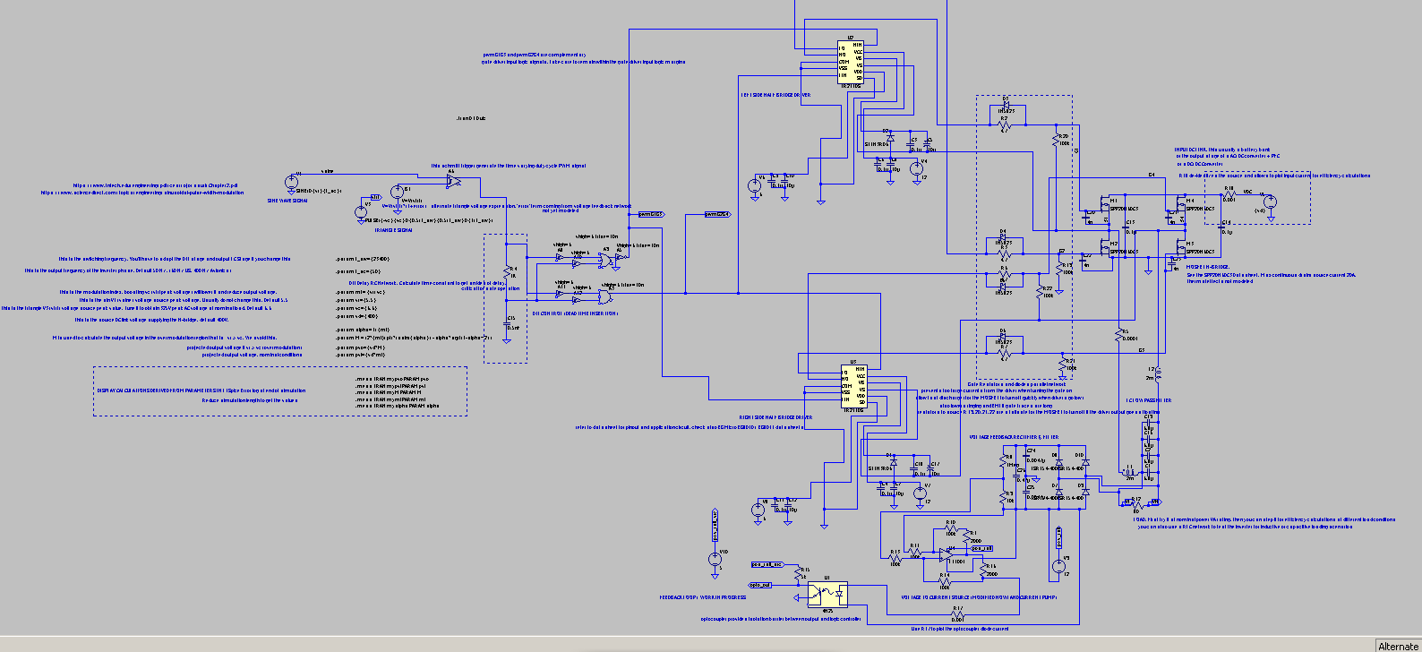
We will provide a hybrid analog/digital LTSpice model for phase synchronisation using the ZCD method.

It is “hybrid” in the sense that the inverter reference sine used in the modulation is phase modulated through a behavioural voltage source, that is more or less equal to what a DDS IC would do, but in a ideal manner since it comes without any quantization noise in LTSpice.

This model will be further updated. Note that phase synchronization using the ZCD method is performed using fully digital means in commercial ASICs. Providing a partially analog method is useful however for teaching analog control and for certain niche cases where the inverter SPWM generation and control feedback cannot be fully automated in the digital domain. (like using an Arduino instead of a fully capable DDS platform), In these cases, offloading part of the control loop to analog components is an option. Generally, fully analog control is less and less used except for simple feedback like in SMPS.

But there are still niche uses, for instance, an environment subject to ionizing radiation where hardening the ASIC is not possible, would be more robust in analog but that would require a fully analog control loop.

How to get phase difference between mains phase and inverter phase using ZCD the analog way ?

The analog ZCD method translates a sine wave (here, the output of the inverter or that of the mains power) into a square wave signal. the rising edge of the square wave signal happens at the upward zero crossing of the phase, and the falling edge at the downward crossing of the phase.

ZC sine to square wave conversion is done both for the mains and inverter phases. This is done using an op-amp comparator without feedback for each phase. The output signal is a square wave with rail to rail voltage levels.

Then, the two square signals are compared using two D type flip-flops, giving outputs pulses widths that are equal to the absolute phase difference information. (it outputs time information, not an angle value)

The method is explained in “Phase measuring circuit with leadlag indication” by Forrest P. Clay Jr. a 1992 electrical engineering paper.

https://sci-hub.ru/10.1119/1.16908

This method preserves the phase lag/lead information. One flip-flop provides HIGH output in leading conditions, While the other provides HIGH output in lagging conditions. Fundamental pulse frequency is the same as the mains and inverter frequency (assuming that both have a frequency deviation that is negligible compared to the nominal frequency) that is, 50 Hz in the model.

Phase difference detector circuit used in the simulation

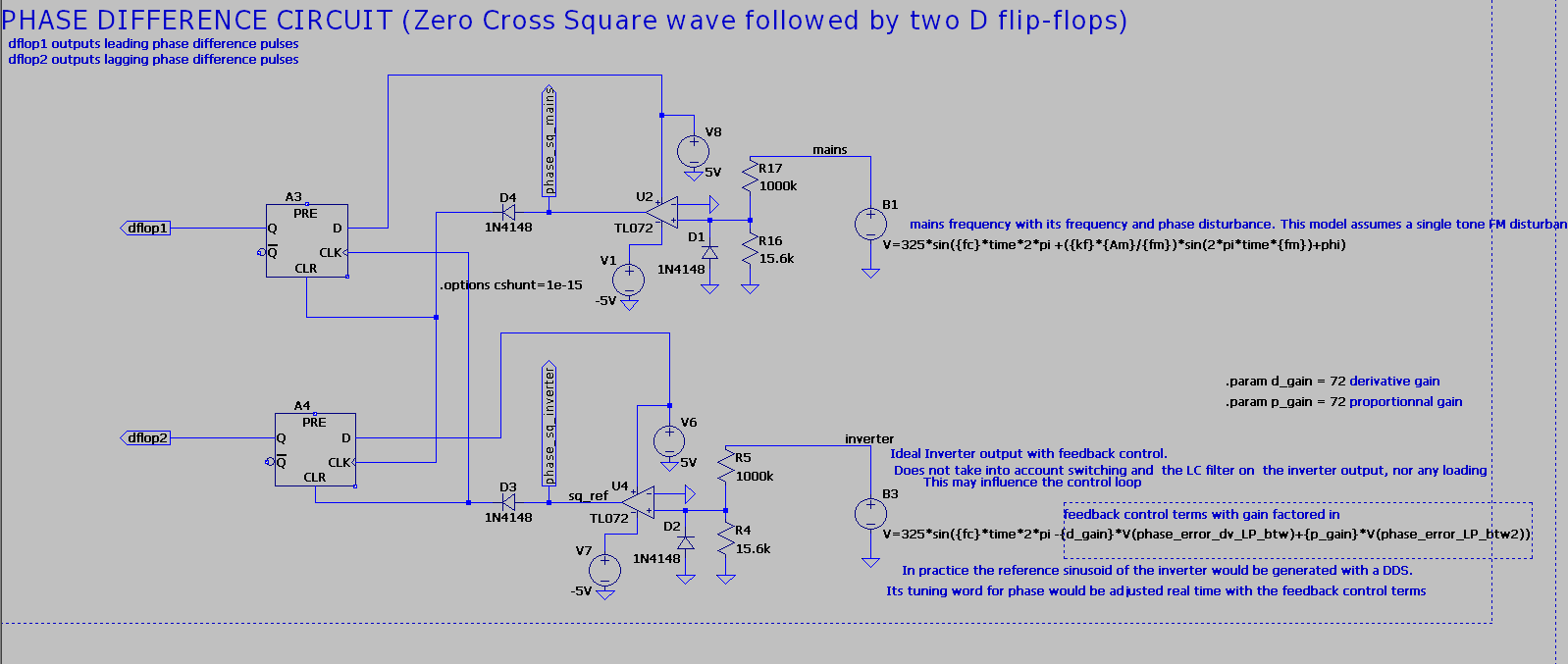
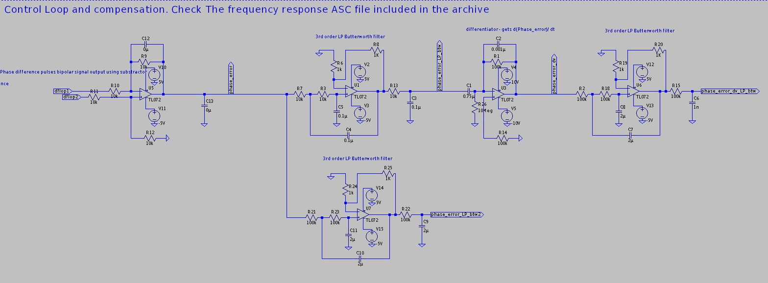
Then, the output from the flip-flops is given to an op-amp substractor that generates a bipolar signal of the phase difference. Positive pulses mean leading while negative pulses mean lagging. Care must be given to the resistors tolerances (1% or better) in a substractor to minimize common mode interference, and a suitable OpAmp for this kind of use is prefered.

This signal is then low pass filtered to remove edge induced discontinuities. Note that usually the mains frequency slew rate is really slow because of the huge rotational inertia of all generators creating the mains distribution network and all regulation mechanisms in place. So it is not a problem to have a filter with a very low cutoff frequency. On the other hand, if the inverter were to synchronize to an islanded generator, that would be a whole different scenario. It is outside the scope of the current article. For these scenarios, other synchronization methods exists, and we named a few at the beginning of the article.

The filter used is an analog 3rd order butterworth LP filter, to get a sharp rolloff. The first stage has a quite high corner frequency, in order to minimize filter phase effects at low frequencies. Its goal is to minimize rising and falling edges coming from the ZCD and flip-flops well enough for the differentiator stage not to complain.

We then get a smoothed phase shift signal $$ \Delta \varphi $$ . This is fed to a differentiator op-amp setup. Its role is to generate the $$ \frac{d(\Delta \varphi )}{dt} $$ signal used further in the control loop. Note that because of processing this signal has a delay, so our notation is a little it abusive.

This signal is further processed using a second 3rd order butterworth LP filter, with a corner frequency way lower than the first butterworth filter. This gets rid of the spikes in the signal. The corner frequency is around 1Hz.

This concludes the generation of the $$ \frac{d(\Delta \varphi )}{dt} $$ processed signal that will be fed to the control loop of the inverter, for the derivative term.

In parallel, we need to get the proportional term. This will use a single butterworth 3rd order LP filter that branches just after the substractor. This will generate the proportional term also fed to the control loop of the inverter. This filter has a lower corner frequency compared to the first LP filter stage used for the differentiator branch.

Note that the final butterworth filter of the derivative signal branch has been slightly tuned out from its canonical form to get an appropriate control loop frequency/phase response.

Other than that, the remaining filters are quite the same. The differentiator has an added C2 capacitor to filter high frequency terms and provide less oscillation.

These two signals (proportional and derivative) are then factored with their respective gains (both are the same in the simulation) and fed as a sum to the behavioural voltage source of the inverter using the phase term of its function.

Note that this is a simplified model of the inverter stage. A more realistic but computationally intensive model would control the sinusoidal reference of the SPWM stage of the inverter, and inverter output would be fed to one leg of the phase difference detector. This would integrate the whole SPWM inverter model to this simulation. Note that this simulation do not include RLC loading of any of the phases. Also, this model supposes that the mains and inverter AC voltages are the same and stable at AC RMS = 230V.

One advantage is that the ZCD method is quite tolerant to voltage variations, compared to methods that are sensitive to it like PLL, So It is not critical to have it factored in this simulation.

Control loop. Not shown the final mixing stage that happens in the BV sine source of the inverter

AC Analysis of the control loop

An open loop AC analysis starting from the input to the first LP butterworth filter up to the output of the sum of the derivative and proportional terms with their respective gains has been performed.

Content of the control loop AC simulation file
Bode plot of the control loop. Plain line is Gain, Dotted line is phase

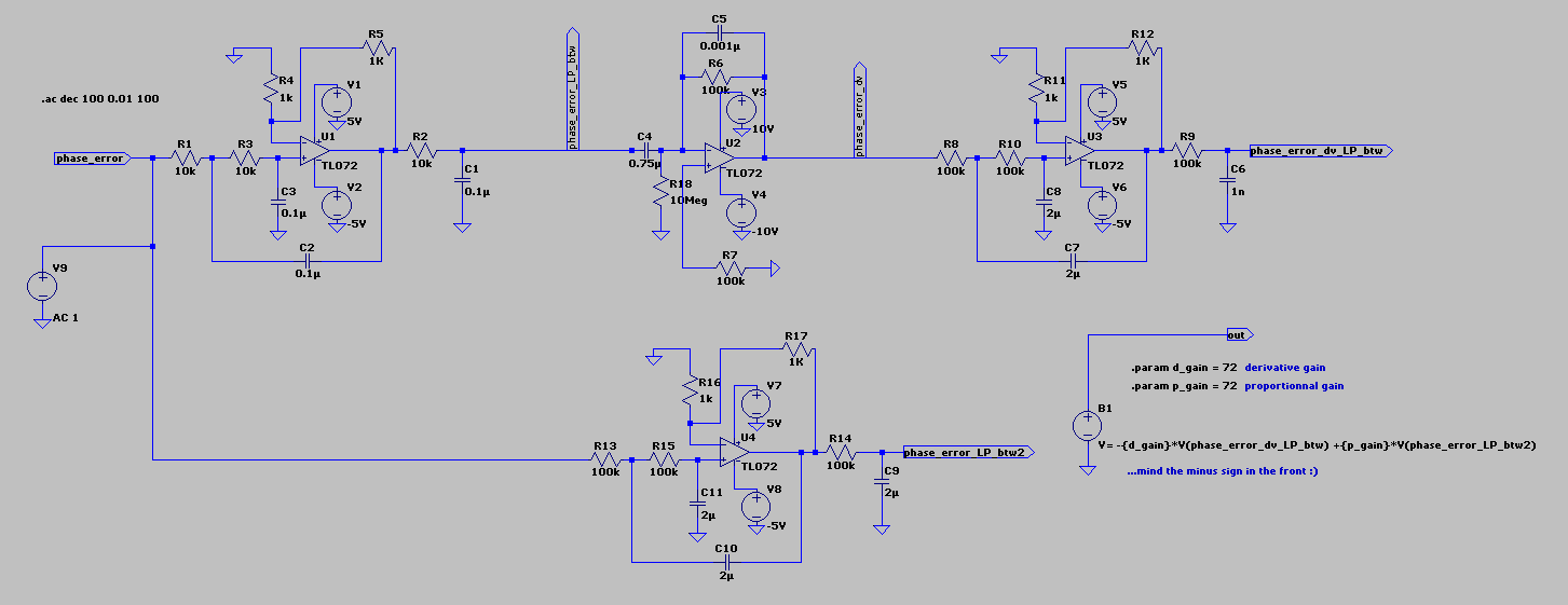
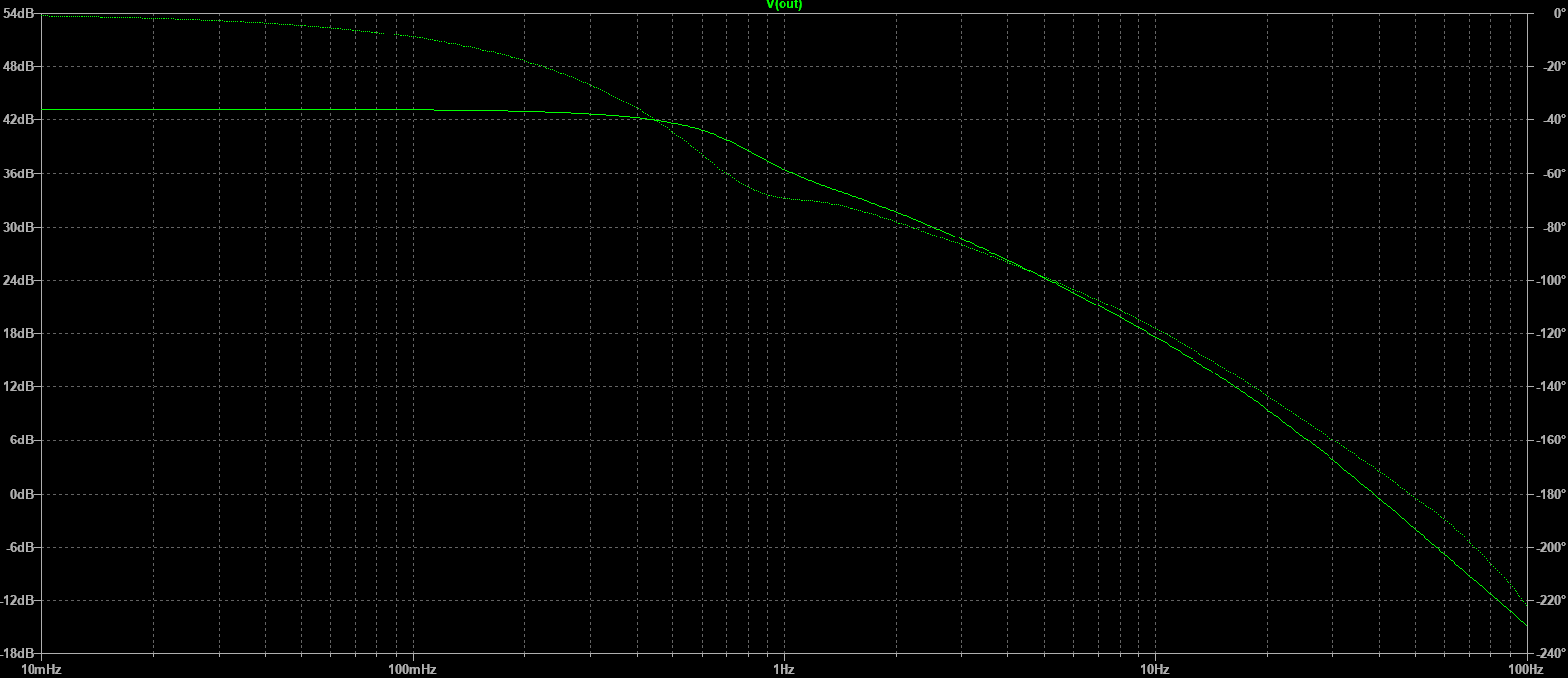
The range of frequency analysis for our first inspection is 0.001 Hz to 100 Hz

The cutoff frequency is approximately 0.66 Hz

The DC Gain is approximately 43.2 dB with a flat response.

Gain margin is -3.5 dB (at f_GM = 48.1 Hz) This could be improved for stability, knowing that this frequency is quite critical being close to the 50 Hz component in the phase difference pulse signal.

Phase Margin is 9.8° degrees (at f_PM = 38.6 Hz). Phase margin could also be boosted. Phase margin stays positive below f_pm.

There is a pole around 0.66 Hz and another close to 1 Hz, barely visible in the plot.

The control loop will be further optimized when I have time. I am no guru of control loops and filters so if you manage to get an optimized model, please chime in using the contact form…

Mains Disturbance simulation

Frequency disturbance

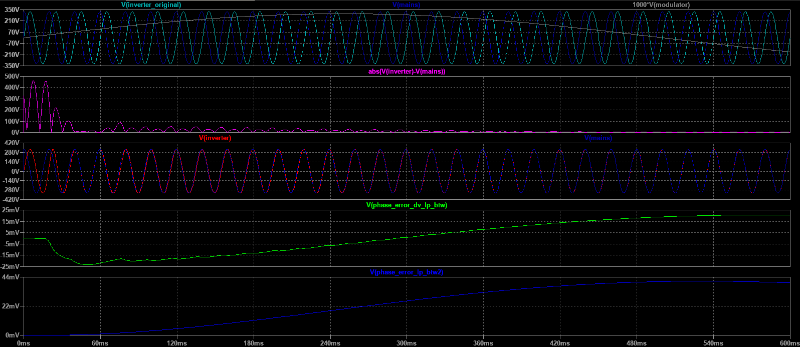
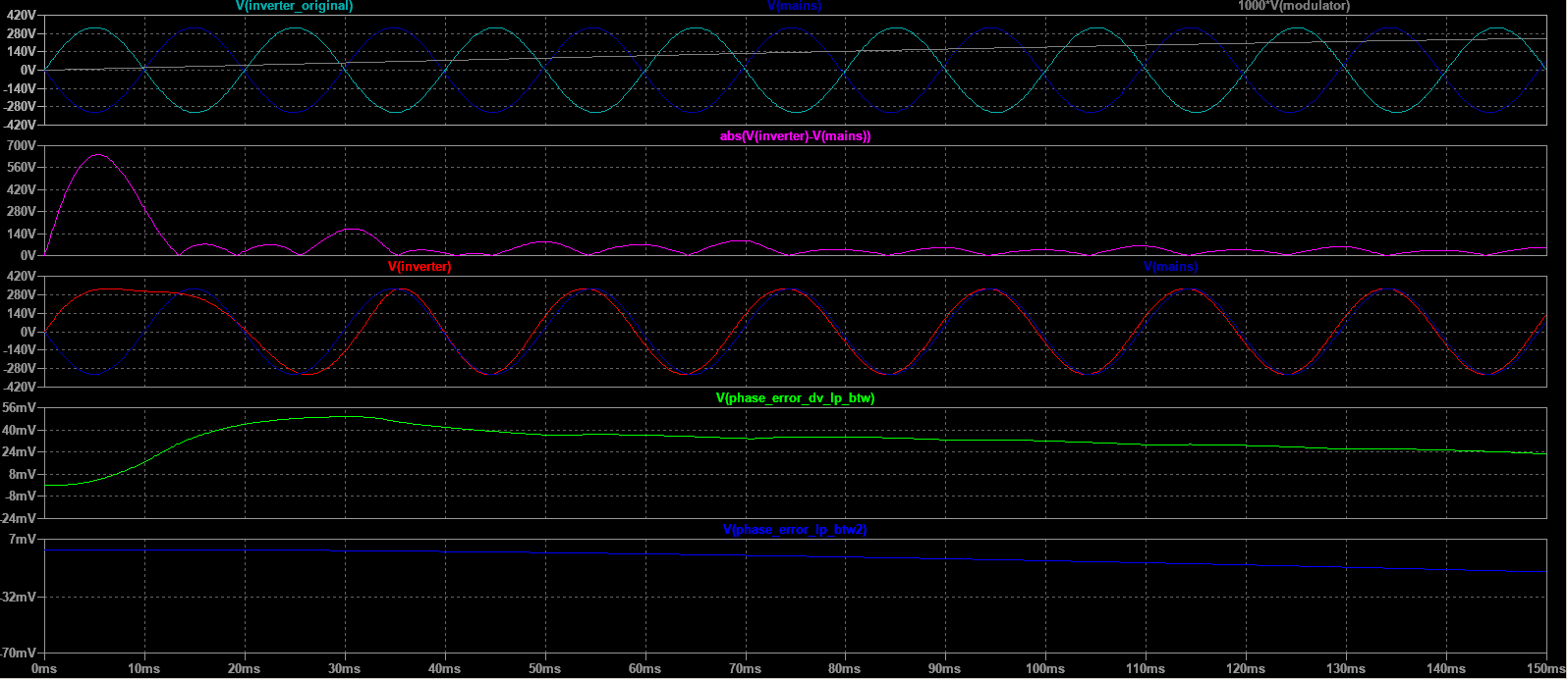
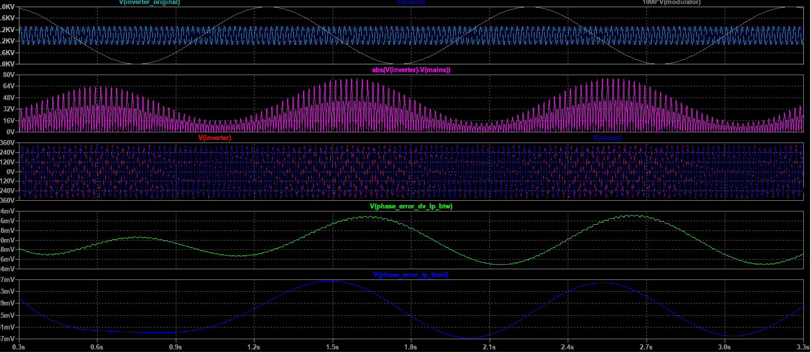
The first goal is to characterize how tightly the inverters locks on the mains frequency that is, $$ min(\Delta \varphi) $$ and $$ max(\Delta \varphi) $$ for a given mains frequency disturbance scenario. We also used a simple function to get an idea of the magnitude of the absolute phase difference by plotting $$ \left | V_{inverter} – V_{mains} \right | $$ and look at the local maxima. note that this plot does not suffer from the delays coming from the LP filters.

Simple FM disturbance

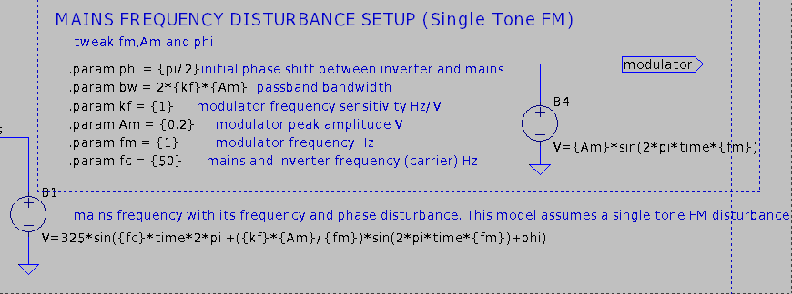
The disturbance scenario modeled this far is a mains frequency oscillation with a parametrized slew rate and oscillation amplitude, using a simple FM modulation scheme. The peak instantaneous frequency deviation will be restricted first to ±0.2 Hz to get in line with the ENTSOE ordinary and contigency frequency deviations, that is, an oscillation between 49.8 and 50.2 Hz

Frequency Stability Evaluation Criteria for the Synchronous Zone of Continental Europe

(section 3, Evaluation Criteria)

https://eepublicdownloads.entsoe.eu/clean-documents/SOC%20documents/RGCE_SPD_frequency_stability_criteria_v10.pdf

There is also this small study from Twente University from 2005 about stability of mains tied clocks.

Accuracy and stability of the 50 Hz mains frequency

https://wwwhome.ewi.utwente.nl/~ptdeboer/misc/mains.html

Since time keeping by these clocks rely on the number of cycles of the mains period, it makes sense to calculate the phase error. This study precisely do this, measuring phase deviations and not only frequency deviations. Phase errors in a power distribution grid come from frequency instability. To compensate for phase errors, an utility company would have to precisely manage frequency compensation at regular intervals to “get back” to the theoretical number of cycles expected. The priority is frequency, not phase, and mains tied clocks are superseded by GPS. However, this anecdotal study is however of special interest since we are dealing with both frequency and phase adjustments in grid synchronization. Note also that an abrupt phase adjustment in a rotational generator such as synchronous machines used in power plants would come from disastrous events such as pole slipping and/or sudden uncompensated load rejection. It should never happen on the scale of an utility grid.

As for the frequency, the slew rate for mains frequency is extremely low in ordinary and even contingency modes, So a rate of 1 Hz is already an extreme worst case scenario. Higher slew rates however happen with islanded generators, but this is outside the goal of this simulation. Given the response of the control loop, low slew rates should not pose a stability problem. However, this depends on the detection threshold of the flip-flop stage. A minimal instantaneous frequency deviation would not be catched until it reaches this threshold.

Note also that frequency deviations include stochastic noise but also predictable deviations according to load consumption and power generation imbalances. Periods of high demand typically introduces a negative frequency deviation until the power generated matches the load power.

As said before, the ZCD method is sensitive to harmonic disturbances typically introduced in non-inverter type islanded generators with low power handling capability relative to load. Thus, further characterizing the control loop for worst case scenarios would need to introduce this kind of disturbance, if one were to use ZCD with generators nonetheless.

Amplitude disturbance

<to_be_continued>

Phase synchronization from arbitrary initial phase difference

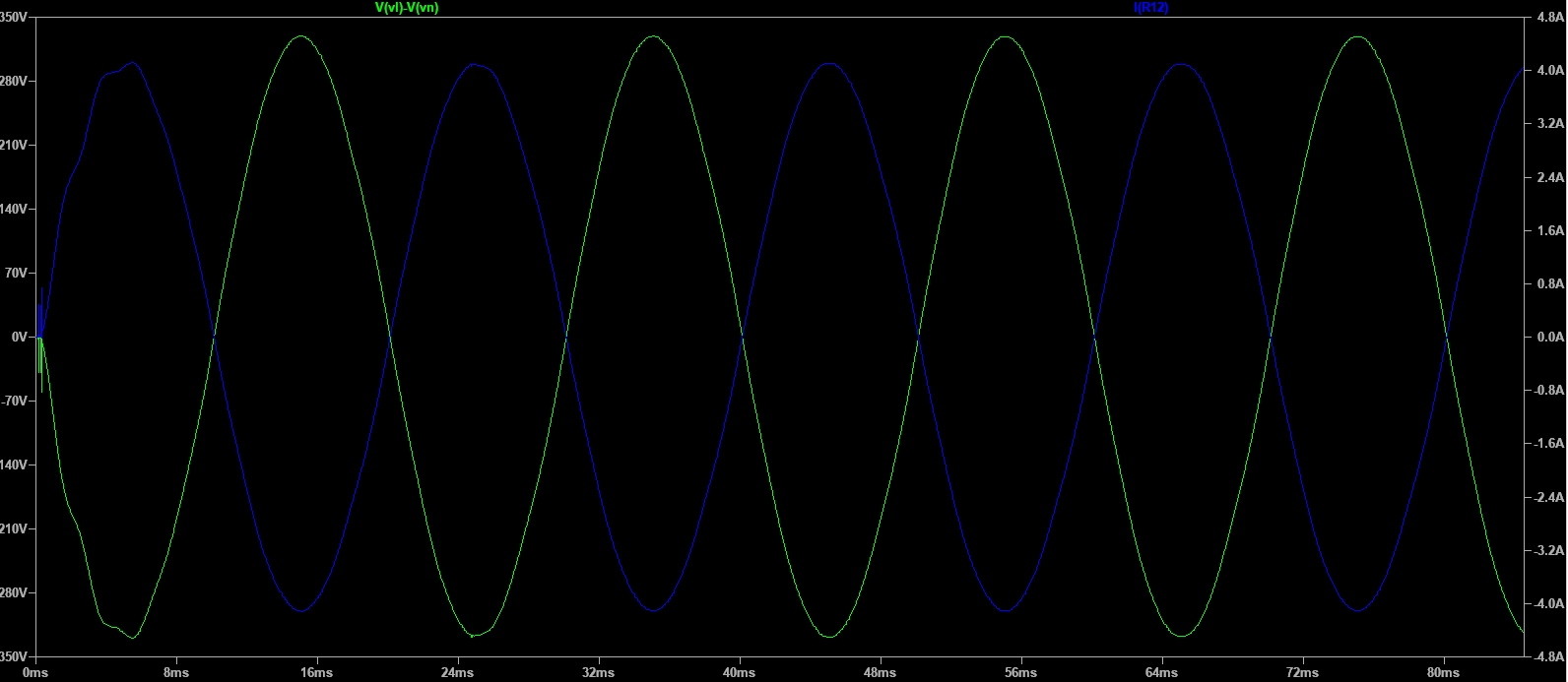
The other goal of the simulation is obviously to track the performance of phase locking from an initial arbitrary phase difference. The inverter has to lock its phase at 0° degrees phase difference from any starting phase difference ranging from -180° to +180° degrees. The performance of this locking process, that is how fast the phases converge to 0° and if the inverter experiences excessive harmonic disturbances during this process will have to be characterized.

Assuming both mains and inverter voltages are of the same amplitude, perfectly sinusoidal, and that the inverters track frequency change instantly or that the simulation is performed at fixed AC mains frequency, performance of phase synchronism can be measured through the following formula, giving the the absolute value of voltage phase difference.

$$ (1)\hspace{1cm} \left | \Delta \varphi \right | = 2arcsin(peak( \frac{\left |V_{mains}(t) – V_{inverter}(t)\right |}{2V_{max}} )) $$

Note that for $$ \left | \Delta \varphi \right | \ll \pi $$

$$ (1a)\hspace{1cm} \left | \Delta \varphi \right | \approx peak( \frac{\left |V_{mains}(t) – V_{inverter}(t)\right |}{V_{max}} ) $$

with peak() defined as the function that returns the peak value as a step function over the time range of interest defined below and

$$ (2)\hspace{1cm} V_{max} $$

the mains and inverter voltage amplitude.

$$ (3)\hspace{1cm} \left [ t_{1} , t_{2} \right ] $$

Since the ‘periodicity’ (the periodicity of the mains frequency induced harmonic component) of the function above is $$ \frac{1}{2f_{mains}} $$, that gives the optimal sample time to extract the maxima when sampling the above function (1)

The above function (1) can be simply plotted. If you need to extract maxima at sampled intervals use these LTspice directives and loop them with subsequent time intervals of $$ \frac{1}{2f_{mains}} $$ and put them into a .MEAS file, although it would need a long simulation time to make sense. For complex data analysis it is better to make a LTspice export of the data and process it with Python for instance.

.meas TRAN Vdiff_abs_norm_max MAX (abs((V(vl) -V(vn)) - V(mains))/(2*1.414*{V_ac}) ) FROM 0ms TO 10ms
.meas TRAN delta_phi_abs_max PARAM 2*asin(Vdiff_abs_norm_max)

measuring the minimum phase difference (best performance at steady state) is less trivial because of zeros in the function when the sine waveforms cross each other, therefore it would require sampling the phase difference with the above method and then analyze the resulting data for local minimums. Overall, another useful metric is simply done by averaging the sampled maximum phase difference (CTRL+click) for function (1) over a long interval, preferably equal to a full oscillatory cycle that arises from the control loop, if one is found.

Finally, performance in phase locking has to be demonstrated in conjunction with a FM disturbed mains frequency.

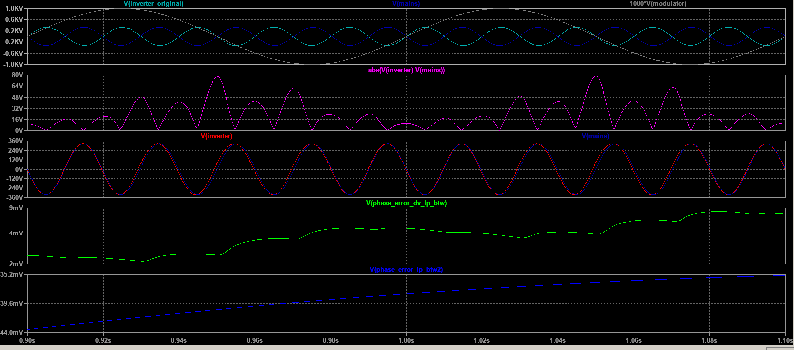
Note that phase locking is preferably done while keeping the waveform sinusoidal in nature during the process. Phase locking in figure 2 happens too quickly, and has the effect of producing severe distortion. The inverter should have adequate protection to not supply power during this event, only after proper phase locking is done. In a mains synchronized double conversion UPS, this could happen if the input is switched between two phases (120°shift) or after the powering on and transfer to a generator. Since a double conversion UPS always provides power through the Inverter stage with no possible downtime except a minimal one for switching to and from bypass mode, the control loop has to be tuned to take that into account. A modification of the phase control term in the sine wave DDS generator could be done and would take effect only during these initialization/switching events, for instance, using

$$ 1-\exp\left(-a\cdot t\right) $$

as a factor of the control term, ‘a’ controlling how fast the control loop locks into the mains phase.

Simulation results

Fig. 1 initial phase difference +90° , frequency disturbance : modulator freq. fm = 1Hz, modulator Amplitude Am = 0.3V
Fig. 2 Initial phase difference +180°, fm disturbance unchanged. Note the large disturbance of inverter phase during the lock process. Locking happens in less than a period
Fig. 3 frequency disturbance : modulator freq. fm = 1Hz, modulator Amplitude Am = 1V
Fig. 4 frequency disturbance : modulator freq. fm = 1Hz, modulator Amplitude Am = 1V At this slew rate of mains frequency and high frequency deviation, performance is degraded.
Fig. 5 frequency disturbance : modulator freq. fm = 1Hz, modulator Amplitude Am = 0.3

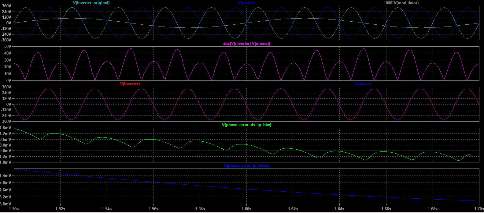
Using the ZCD method, sampling time is limited at two times the mains AC frequency. That limits accuracy of the algorithm for fast and ample disturbances. But a heavily distorted power source would not lead to any application requiring syncing into it, rendering that issue moot.

On the other hand, ZCD is quite tolerant to voltage fluctuations.

Conclusion

Although this controller is simple to implement, it suffers from steady state error due to the limited gain at DC. One option to mitigate this is to add an integral component. However, it would still suffer from delayed response to oscillations due to the butterworth filters, and cannot track fast oscillations. The ZCD+Flip Flop stage also samples phase at 1/2*f_ac, which is a limiting factor. The non linear behaviour introduced by the discrete function of the flip flops, who encode phase difference as a pulse further make the tuning of the control loop harder, with the need to analyze the impulse response of the system. However the discrete ZCD phase difference method is more robust when it comes to voltage imbalance between the two measured phases.

In a next post, we will propose a time continuous control of phase difference without flip-flops in the control loop signal path (although one is still needed in the circuit).

To get back to the conclusion on this model : Its performance level is unacceptable for grid tie operations, nor it provides the required functions and behaviour of GFL,GFM,GS grid tie topologies. That is why we limit it to synchronization for inverter standby/autonomous operation to alleviate source switching transients. But it is a good introduction on the subject. For an idea, it is closer to the state of the art for the start of the 90s or so, when digital control was not yet so widespread.

We will discuss grid tie inverters in a later post and slowly but surely move into the more state of the art technologies. It will also serve as an introduction into fully closed loop control systems, as with grid tie inverters, voltage,current quantities are intimately tied, and reactive power effects have to be taken into account.

Beware, the learning curve will be steep.

Simulation files

EGMicro EGS005 board review

The goal of this post is to analyze in detail the advertised features of the EGS005 board, and show possible modding hacks.

The EGS005 board is the newest board provided by EGMicro for single phase and multiphase inverter designs.

It is based on the EG8025 ASIC that features integrated MOSFET drivers for a full bridge configuration.

Most if not all all of the EGS005 information is also provided in the EG8025 datasheet, plus many more details! We will use the EG8025 datasheet as the reference material, but also compare them to the EGS005 board features, to see what features are restricted by the board.

The EG8025 datasheet is available on the EGMicro website, chip center section.

Probable IC orientation

Pinout analysis and IC orientation.

Based on the application schematic and components names and indexes placement, and after boosting trace contrast, it seems pretty evident that this is the ASIC orientation on the EGS005. The D4, D5 diodes and the C17 capacitor with its traces clearly shown going up to the pin, plus the 3 NC pins at the bottom and at the right side make it the only possible configuration. This setup would make the pin1 orientation dot in the product image misleading.

Differences between EGS002 boards and EGS005 boards

We will focus our attention first to the differences in features between these two boards. This takes into account only the features exposed through these two boards, not the overall feature differenciation between EG8010 and EG8025.

EGS005 has these additional features compared to EGS002 :

  • integrated MOSFET drivers
  • Test mode for SPWM output bench testing without any control loop feedback
  • overload protection (not only overcurrent hard limit)
  • Two over temperature control zones (IGBT/MOSFET and PCB)
  • SPWM signals routing swap on/off between left bridge and right bridge MOSFETs
  • AC output enable/disable through pin (basically a soft shutdown)
  • Exposed Serial interface (RX and TX), but configuration settings registers besides switching in and out of “Test mode” are either unavailable or undocumented.
  • Exposed pins for firmware update

EGS005 features that are discontinued compared to EGS002 :

  • Variable frequency output mode up to 100Hz or up to 400Hz. This includes variable frequency mode and fixed ratio V/F mode.
  • Choosing between unipolar and bipolar SPWM. Note that EG8025 supports phase synchronisation/phase shift for 3 phase mode, so the modulation scheme had to be made unique for interoperability.

EG8025 features not exposed in EGS005 :

  • Phase shift mode for AC sensing from another unit – Phase_SEL pin 12
  • AC input for phase synchronization/shift from another unit – VZC_IN pin 17
  • AC output for phase synchronization to another unit – AC_Fout pin 13
  • Multi inverter pin for parallel operation or master/slave select for three phase operation – Multi_INV pin 15

Inverter phase synchronization and phase shifting

Inverter phase synchronization is required for the following operation modes.

  • Parallel mode of operation of two or more inverters sharing a single phase for load sharing / redundancy.
  • Parallel mode of operation between one or more inverters and the AC grid, These inverters are known as Grid tie inverters. They are ubiquitous in renewable energy systems for residential or industrial use.
  • Parallel mode of operation between inverters or between inverters and AC grid, who do not share the load for redundancy (active/standby system). The phase is kept synchronized between the sources for seamless operation of an ATS (Automatic Transfer Switch). This is to limit potentially high dV/dt (and/or high dI/dt) that happen during switching when the phases are not synchronized.
  • Multiphase mode and inverter daisy chaining (cascade) of phase synchronization across usually three units, for three phase power applications, In a (master)/(slave/master)/(slave) configuration. Parentheses correspond to the three inverters.

There are several digital algorithms and analog tehcniques to implement phase synchronization.

One well known and ubiquitous method used in various electronics designs not limited to inverters is PLL (Phase locked loop). There are however other methods. This paper discusses them in detail :

Recent advances in synchronization techniques for grid-tied PV system: A review

https://www.sciencedirect.com/science/article/pii/S2352484721008118

EG8025 Phase synchronization

The EG8025 ASIC uses the Zero Crossing method. It is simple and straightforward.

It uses 2 pins for configuration. Multi_INV pin 15 and Phase_SEL pin 12 and 2 pins for synchronization data. One is an output pin, AC_Fout pin 13 the other is an input pin VZC_In pin 17.

Parallel operation mode

We’ll assume that we use two inverters.

In this mode both inverters share the load on the same phase. One unit is designed as master and has Multi_INV pin 15 pulled log to GND, The other is designed as slave and has Multi_INV pin 15 pulled high to 5V.

The master unit also has VZC_In pin 17 and Phase_Sel pin 12 pulled to GND. Since the master is the start of the synchronization chain, it won’t use an input ZC signal, nor it should shift the phase 120° for parallel operation. Applying phase shift in this mode of operation could destroy both inverters output stages !

The master outputs its phase information through the AC_Fout pin 13. This is a zero-crossing signal. It probably converts upward going zero-crossings of the AC phase to logical HIGH, and downward going zero-crossings of the AC phase to logical LOW. Rising/Falling edges should happen at the time of the zero crossings. Checking precisely the logical levels correspondence is required if this board is to work with another unit of another manufacturer supporting ZC synchronization, to prevent a 180° out of phase condition. Level shifting may be required to accomodate the slave unit.

The slave in turns gets its ZC information on the VZC_In pin 17. The path between AC_Fout pin 13 of the master and VZC_In pin 17 is isolated with the use of an optocoupler. Check figure 10.a of the 8025 ASIC Datasheet. On the slave unit Phase_Sel pin 12 is also pulled to ground while AC_Fout pin 13 is floating.

Since AC_Fout is a low impedance pin current source, it should never get pulled to GND.

Modding for parallel operation.

We should investigate the board and the EGS005 application schematic to look at the trace routing of VZC_In, AC_Fout, and Multi_INV.

Modding fo the slave unit :

  • VZC_In is pulled to GND through the R45 1k resistor. Making the VZC_In as an input as shown in figure 10.a would require soldering out the R45 resistor and supplying the signal to the exposed pad of R45 connected to the pin. This signal comes from the optocoupler voltage follower.
  • AC_Fout and Phase_Sel do not need any mod on the slave unit.
  • Multi_INV trace to GND should be cut and a patch wire soldered and connected to 5V HIGH level

Modding fo the master unit :

  • AC_Fout is floating on the EGS005 so a simple wire patch to the pin would do the trick. This wire would be routed to the optocoupler diode anode.
  • Multi_INV and Phase_Sel do not need any mod on the master unit.

For a tutorial on how to perform SMD pcb wire hooking look at :

EGMicro EGS002 board review

The goal of this post is to analyze in detail the advertised features of the EGS002 board, and show possible modding hacks.

The EGS002 board is the oldest provided by the EGMicro supplier still distributed on common Chinese reseller platforms. It superseded the even older EGS001.

It is based on the EG8010 ASIC and also features either two IR2110S half bridge drivers, or two EG2113, an EGMicro driver. Whether you get one or the other depends on the reseller. Check for comments and reviews on marketplace product page to see who’s getting what.

Most if not all all of the EGS002 information is also provided in the EG8010 datasheet, plus many more details! We will use the EG8010 datasheet as the reference material, but also compare them to the EGS002 board features, to see what features are restricted by the board.

EG8010 ASIC Features

Input DC Voltage. The EGS002 can drive high voltage MOSFETs easily. no restrictive voltage limitations on the high side MOSFETs, and it is at least ok for 400V DC input to the MOSFET bridge. Supplied design schematics show power coming through a 400V DC link PFC output.

Inverter output frequency. EG8010 can be used for fixed 50Hz,60Hz or frequency adjustable 0~100Hz or 0~400Hz output.

The EGS002 on the other hand restricts this feature to fixed frequency operation : either 50Hz or 60Hz, through jumpers.

These jumpers are exposed on the bottom plane of the board and are set with solder bridges over two pads. They do not appear to be through hole, so it would be difficult to insert header pins and use a real jumper there.

the backside exposes the configuration jumpers. top left of image

JP1 and JP5 on the board control FREQSEL0 pin 18 level (either HIGH=JP1 short for 60Hz or LOW=JP5 short for 50Hz). They can’t be short or open at the same time !!

Is the board moddable for further frequency control ? let’s see.

There seems to be two methods to apply mods. Either through hardware or through software (by serial commands). Let’s explore the hardware method first.

Variable Frequency mode modification

Up to 100Hz or up to 400Hz variable frequency operation mode selection is controlled by FREQSEL1. It seems however that the EGS002 has the FREQSEL1 pin 19 grounded in the EGS002 schematic. So it depends on the suppliers of EGS002 to create derivative boards that expose FREQSEL1.

As far as I searched on Chinese marketplaces that doesn’t seem to be the case.

PIN 19 and PIN 20 Traces Merge. right around the center of R33. Processed image to better expose the traces

FREQSEL1 pin 19 and MODSEL pin 20. seem both connected to ground in most boards available on the market through merging traces. This is in conformity with the EGS002 datasheet.

That restricts the unmodded board to 50/60 Hz Operation and Unipolar switching

Modding for tests to enable VVVF to 100 Hz or to 400 Hz would require cutting the FREQSEL1 pin trace and patching the pin with maybe AWG30 hookup wires and connect it to HIGH level. MODSEL would be still kept to GND.

JP1 and JP5 would allow to control max frequency to 100Hz or 400Hz.

Note that variable frequency with constant voltage mode and variable frequency with variable voltage both require Unipolar switching. That is why you don’t have to bother with MODSEL in this mod

Once FREQSEL1 is set to HIGH, Variable frequency mode type is enabled through VVVF pin 32. In EGS002 again, it is connected to ground. This mode would give EGS002 the variable frequency constant voltage mode by default. (without further mods)

To enable VVVF variable freq/variable voltage (albeit with constant V/F ratio) for single phase VFD applications, bring VVVF to HIGH

Pin 32 VVVF. For variable frequency mode in unipolar switching

Again, the trace after the pin may be cut if other pins do not depend on the cut trace, which may be difficult to check since some trace may hide under the IC.

Note that there are several test points / open vias on the board that can be used to patch the board with additional connections.

Then you have to expose FRQADJ/VFB2 pin to set the desired frequency in variable frequency mode through an external potentiometer in figure 8.6a of the datasheet. Voltage regulation is still performed through R23 and VFB1

In constant voltage/frequency ratio mode, you use R23 to set the nominal voltage at 50Hz through VFB1 Frequency ratio control goes through FRQADJ/VFB2 in this mode. It is a bit unclear in the datasheet.

Bipolar SPWM enable modification

Remember that you cannot use VVVF features in this mode.

The mod would require :

  • cutting MODSEL pin 20 trace to disconnect from ground and patch it logic HIGH.
  • cutting FRQADJ/VFB2 pin 16 trace/pad to disconnect it from ground and use it to supply voltage feedback as shown in the EG8010 bipolar switching application schematic. In this mode VFB pin 13 and FRQADJ/VFB2 pin 16 are supplied a differential voltage feedback. It is required in bipolar switching. .

However, all boards found on the market seem to implement the application schematic “Figure 6‐2. EG8010+IR2110S+cross‐conduction prevention logic sinusoid inverter(unipolar modulation)”

The cross conduction prevention logic is inserted between the ASIC logic outputs and the Gate drivers logic inputs. It consists of resistors and BJTs

I think that would prevent the bipolar SPWM mode from working. So you need further modding.

  • You need to unsolder Q2 Q3 Q4 Q5 and solder bridge collector and emitter pads.
  • Remove resistors R30 to R37

Using the UART to set the operation modes

The ASIC also exposes an USART interface (RX pin 4 and TX pin 5)

The data inteface looks powerful, exposing all configuration options usually set by the jumpers. Whether the override of the jumpers is properly done by the USART remains to be seen.

Note than enabling bipolar SPWM would still require the removal of the cross conduction prevention components.

It also allows for monitoring the same parameters than in the LCD Output, that is frequency, current, temperature, and voltage.

The EGS002 has the RX pin to GND and the TX pin floating, Again cutting the trace to GND could allow to access to the USART. The data interface is fortunately documented in the datasheet. it uses 2400,8,N,1 serial settings.

Dead Time Control

EGS002 implement dead time control through solder bridges at the bottom layer of the board. These are JP3, JP4, JP7 and JP8.

The EG8010 has a fixed switching frequency of 23400 Hz that makes a pulse at 50% duty cycle time duration of roughly 21µs.

That makes the ratio of dead time to pulse length quite important at 1.0 and 1.5 µs, and may impact scaling up for higher output power. The default is 300µs. That is still quite conservative.

Check your MOSFET specifications for minimum dead time requirements.

Soft start

EGS002 has a soft start 3 second feature enabled by default through JP2. I do not recommend disabling this feature.

Voltage feedback & regulation.

It doesn’t look like there are any rectification on the voltage feedback network, nor on the EGS board or outside. and the RC filter made with R4 and C4 has a small time constant of 1ms. The voltage regulation uses a peak detector and measures error in relation to a 3V reference as per datasheet.

In any case the voltage nominal setpoint is performed through the lower leg of the voltage divider using R23 (a 10K potentiometer). A slow acting external voltage control could be done by replacing R23 with a current DAC.

Bipolar switching voltage regulation

You will see in the EG8010 datasheet that the voltage divider network is more complex (it is outside the ASIC board) than for unipolar, with a ganged potentiometer R23. I also suspect missing connection dots in the schematic between R19 and R21 and also R26 and R27 and also at R27 low leg and GND.I will test it on my LTSpice model, so take that info with a grain of salt. Here is the relevant section of the schematic with the proper corrections

bipolar switching voltage divider

Overcurrent protection.

The method employed is a hard current limiter. It cuts the SPWM input to all MOSFET drivers if the output current goes above the setpoint for more than 600ms. The unit is shutdown for 16s, then it will turn on for 100 ms, check for current status and repeat that 100ms on time every 16s if the issue persists for a maximum number of 5 cycles. if the issues persists it powers off and a hard reset is required. If the issue is cleared for more than 1 minute, the state machine resets overcurrent status to nominal.

The board also uses a LM393 OpAmp to process the IFB feedback to shutdown the Gate drivers directly through their SD pins, it is much faster and failsafe than doing this only through the ASIC.

There does not seem to be any soft limiter for light or moderate overcurrent protection (that would lower load voltage for resistive and inductive loads)

A soft limiter would not help for Active loads such as AC/DC PSUs because they change their apparent impedance to compensate for voltage loss.

Monitoring and UI

The monitoring is done through a LCD interface using I2C LCD compatible modules specified in the datasheet to display basic information. Or it can be done through the serial link if you expose the pins properly.

400V DC to 230V AC pure sine wave inverter model using LTSpice.

Ltspice inverter model

Note : the above model has been updated for frequency/phase synchronization. please check :

output voltage and current waveform, 80 ohms resistive load
Disclaimer : This design uses dangerous AC and DC voltages. If you get out of the simulation domain and start prototyping be sure to use all safety precautions required when working with high voltages. You have to know what you are doing.

Besides the simulation this post is an introduction on pure sine inverter technology targeted at electronics engineers that have little or moderate experience in power electronics and inverter design.

The goal is to design, implement and prototype your own pure sine wave inverter from scratch as an educational project to get into inverter technology, this will be the object of a series of posts in the future.

For a faster design approach see the bottom of this post on how to use off the shelf inverter modules such as EGS002 or EGS005 available on BangGood and AliExpress.

To get straight into the model simulation go to the running the simulation section.

Introduction

Inverters use MOSFETS to switch a DC source with a variable duty cycle PWM signal.

The duty cycle variation in the time domain is performed at the frequency of the required output fundamental frequency of the inverter.
Usually mains frequency, that is 50hz or 60hz.

The frequency of switching, that is the frequency of the PWM signal is called the switching frequency. it is usually in the 2.5khz to 100khz range.

So, the goal is to have a PWM signal at high frequency (2.5 khz to 100khz) with a variable duty cycle whose frequency is at mains frequency.

However, The variable duty cycle frequency may be lower or higher, or can be adjusted in real time.

Applications that require this duty cycle modulation at fixed but non standard 50Hz or 60hz are mainly for the aerospatial industry.

Airplanes use 400hz. The advantage of 400hz is that power transformers are less bulky than in 50Hz.

There is also an industry need to adjust the inverter output frequency in real time. This is the market segment of VFDs (Variable Frequency Drive) inverters.

This allows to set the rotation speed of induction motors, and allow for a soft-start that does not damage the motor.

In VFD applications, not only the the frequency output of the inverter is managed, but also the output voltage, and sometimes they implement a fixed voltage to frequency ratio mode so the motor stays happy.

So, now comes the question, How to modulate the duty cycle of a PWM signal ?

This is usually done by comparing a triangle signal at the switching frequency with a reference sinusoidal signal at the desired mains frequency.

This can be done in two ways :

1) Using analog components : a sine generator IC (like the XR-2206 or MAX038) that outputs a triangle wave and another one (also XR-2206 or MAX038) that outputs the sine wave. Then, a schmitt trigger is used to compare these two signals to output a PWM signal.

2) Using digital components : the sine modulated variable duty cycle PWM output is generated by code running on MCUs, PIC, DDS IC. Arduino can do this, however Arduino has a limitation that hinders its use for this purpose, and that is dead time control. More on this later.

If you nonetheless want to experiment with SPWM generation with an Arduino, check this code to get an idea of how it works.

I recommend you read resources on Fast PWM for Arduino. It is not straightforward if you have no experience with hardware counters/timers. Check https://www.arxterra.com/tutorial-on-fast-pulse-width-modulation/ and https://docs.arduino.cc/tutorials/generic/secrets-of-arduino-pwm
for starters. You may have to browser for other resources because I could not find one comprehensive documentation for ALL modes, except maybe in AtMel datasheets, but these are very terse and quite hard to understand.

Here is the first code sample :
#include <Arduino.h>

uint16_t freq = 50; // inverter output frequency
uint32_t counter = 0;
uint16_t mod_index = 0.9; // modulation index. you will have to update this in real time for precise voltage control.
float sin_val;
const uint16_t samples_per_period = 100; 
// higher samples per period give a better looking output sine wave, less harmonics from digital aliasing
uint16_t micros_interval;

uint16_t sin_table[samples_per_period];

void populate_sin_table() 
{

  uint16_t i;
  for(i=0;i<samples_per_period;i++)
  {
      sin_val = 512*(1 + mod_index*sin(2*PI*float(i)/samples_per_period));
      sin_table[i] = round(sin_val);
      //Serial.println(int(sin_val));
  }

}

// FAST PWM PHASE-CORRECT MODE 3

void setup(){ 
   
  // Wave Form Generator: phase correct PWM mode 3, Top = OCR1A and OCR1B
  // We will output two signals, complementary, using two pins ~9 and ~10 so we need to specify
  // (0<<COM1A0) + (1<<COM1A1) + (1<<COM1B0) + (1<<COM1B1)
  // (0<<CS10) + (1<<CS11) + (0<<CS12) this is the prescaler and will dictate the switching frequency.
  // (1<<WGM11) + (1<<WGM10); and (0<<WGM13) + (0<<WGM12) are used to set the Fast PWM mode, here we use mode 3.
  // it allows a 10 bit amplitude resolution for the sine wave signal
  // check this link for a table of available modes.


  TCCR1A = (0<<COM1A0) + (1<<COM1A1) + (1<<COM1B0) + (1<<COM1B1) + (1<<WGM11) + (1<<WGM10);
  TCCR1B = (0<<WGM13) + (0<<WGM12) + (0<<CS10) + (1<<CS11) + (0<<CS12); 
  
  OCR1A = 0x3FF; // top compare value initialization. it will be varied using the sine table in the loop.
  OCR1B = 0x3FF; // same for the second PWM signal
  
  //DDRB |= (1<<PB1);

  //Serial.begin(9600);
  populate_sin_table(); // create a sine table. better use PGM write and store it in flash for a more robust approach
  micros_interval = int(float(1E6)/(float(freq)*float(samples_per_period))); // the loop wait delay between two bit bangings
  // of OCR1A and OCR1B.

  //Serial.println(micros_interval);
  
} 


void loop() { 
 delayMicroseconds(micros_interval);
 OCR1A =  sin_table[counter%samples_per_period]; // iterate on the sine table, use modulo to loop the table
 OCR1B =  sin_table[counter%samples_per_period]; // same for the second SPWM
 
 //Serial.println(sin_table[counter%samples_per_period]);
 //Serial.flush();
 counter++; // overflow not managed !!!!!
} 

There is also this wonderful code https://forum.arduino.cc/t/dead-time-between-pwm-signals/937405 for a three phase system. I did not test it but it looks serious and legit. It has the advantage of using ISR and not a loop to update the TOP value with the sine wave, generates 6 signals (so it is for bipolar spwm) but it suffers from the same dead time insertion problem however, and that is the object of the guy’s post. But it is possible with analog post processing, check the DTI section.

That is why STM32 based boards are better for an all digital SPWM generation purpose, but they are more expensive and you'll need to watch quite a bunch of tutorials to master Nucleo (the STMicroelectronics MCU IDE). It will be easier if you already master Arduino FastPWM generation, but it will require time nevertheless.

Now is a good time to learn about the specifics on how that sine modulated variable duty cycle PWM signal allows the inverter to generate a 50hz, 60hz or higher frequency mains power phase voltage.

The "sine modulated variable duty cycle PWM signal" will be now referred by its usual name in the power electronics technology as SPWM (sine PWM)

The power core : the MOSFET H-bridge

The power core of an inverter uses an H-bridge configuration because the setup of its components ressembles to the letter H.
It is one of the most common designs in the industry.

MOSFETs switch repeateadly a DC source with low source impedance (the power source) according to the input gate signal that comes from the SPWM.

That is not all. high VDS high current MOSFETS usually need gate voltages that are higher than what an MCU or an analog oscillator can generate.
The high side MOSFET gates  of the H-bridge also need voltages with reference to DC ground that are way above the levels of the logic/analog controllers.

For that reason, there is a specific family of ICs that exists and they are called "MOSFET Gate Drivers". Their goal is to bridge the gap between the logic SPWM signals and the required voltage levels (and current requirements) of the MOSFET gates.

Moreover, an H-bridge inverter has at least 4 mosfets. These MOSFETS need to be activated by gate signals at a precise fashion, like a fine tuned choregraphy.

The activation pattern is usually diagonal in the schematics. This has the effect of reversing the polarity with reference to DC GND seen by the load with each pwm pulse. Since the two SPWM signals are complementary in this design, when one diagonal set of MOSFETs has a high duty cycle it will be on and conduct a longer time than the reciprocal diagonal set of MOSFET, when this happens the output sine wave of the inverter is at a +Vo_peak. Then there is a time when the duty cycle 0.5 for both diagonal pairs, at this point the sinusoidal output of the inverter crosses 0V. then the cycle goes in the reverse direction and outout reaches -Vo_peak.


PWM Modulation schemes

I just described one SPWM modulation scheme. There are two schemes that are most commonly used.

- Unipolar SPWM
- Bipolar SPWM

To understand the difference between the two, please read now :

https://www.sciencedirect.com/topics/engineering/sinusoidal-pulse-width-modulation
https://www.tntech.edu/engineering/pdf/cesr/ojo/asuri/Chapter2.pdf

My guide is based on Bipolar SPWM.

As you may already guessed, for that SPWM scheme you need two complementary SPWM signals.
For analog SPWM generation, the original SPWM signal generated from the triangle to sine comparator is fed to a NOT gate to create a complementary SPWM signal.

The original signal will drive the Top Left MOSFET and Bottom Right MOSFET
While the complementary signal will drive the Top Right MSOFET and Bottom Left MOSFET.

Note that in an unipolar SPWM scheme, The complementary SPWM signal stays low the whole time the other one operates, and then starts doing SPWM modulation while the other one stays quiet. This switching happens at 2*f_mains,
I find it harder to generate these two kinds of SPWM signals using digital means, so I think that the bipolar scheme is better to start grasping the technology.

Note also that IC Gate Drivers usually manage two MOSFET for a half bridge configuration. So we need Two gate driver ICs
In the LTSpice model IR2110 is used, as it is quite common in the industry.

The routing between the SPWM signals and gate drivers is as follows in my LTSPICE schematic and simulation :

SPWM signal is provided to HIN input of Gate Driver 1 and LIN of gate Driver 2
Whereas the complementary SPWM signal is provided to LIN input of gate driver 1 and HIN input of gate driver 2

HO output of gate driver 1 drives the top left M1 Mosfet
LO output of gate driver 1 drives the bottom left M2 Mosfet
HO output of gate driver 2 driver the top right M4 Mosfet
LO output of gate driver 2 drives the bottom right M3 Mosfet.

If you connect the dots, you'll see it fits the requirements of bipolar SPWM modulation scheme.

The big issue : dead time control.

There is a factor that needs extra precautions because it can fry the MOSFETs and brick the inverter. In no case, the M1 M2 MOSFETs should conduct at the same time.
This also true for M4 M3. If that would happen, The low impedance DC source will short through these MOSFETs (from Vdc to GND). When driven to high gate voltages, these Power MOSFETs  have a ridiculously low RdsOn, This will generate currents way above the absolute ratings of the MOSFET, frying them if a DC breaker or another protection from the upstream DC link did not catch it in time.

For this reason, a security margin between the two SPWM signals (the original and complementary) has to be put in place, This is a delay between pulses where both SPWM signals remain low. This is called dead time.

a good article to read on that subject :

https://hackaday.io/project/3176-gator-quad/log/11741-pwm-control-and-dead-time-insertion

For digital SPWM generation, forget about Arduino to get SPWM plus dead time control using Phase correct PWM out of the box.
Better PICs or MCUs are required such as STM32.

It is however possible to apply analog treatment to a single SPWM arduino generated signal, to create a complementary signal with a dead time delay inserted before the rising edge and after the falling edge.

In the supplied schematic, it is done through a RC network whose time constant is matched to introduce the required dead time, plus a bunch of gates and schmitt triggers. This setup may be simplified, if you manage to use less components or update the model to use real world components instead of ideal ones, let me know through the contact form.

Output Voltage control and regulation.

Output voltage control of the power stage is performed basically by varying the triangle peak voltage, while the sine voltage remains the same.

The peak output voltage is roughly given by 
Vo_peak = V(dc)*V(sine)/V(tri)
Vo_RMS is then V(dc)*(V(sine)/V(tri))/sqrt(2)
V(sine)/V(tri) is known as the modulation index (mi) 
it is usually < 1

If V(sine) gets larger than V(tri), the inverter operates in the overmodulating region, and RMS output voltage is no longer linearly dependent on V(dc)
It appears in the simulation as a voltage saturation of the output.

overmodulation is outside the scope of this guide but it is explained in the above mentioned resources.

An open loop control is not realistic because of deviations from theory that assumes ideal components, and dependance on the load RLC parameters and the output filter parameters, as well of the transformer if an isolated output is required. 

So there is a need for a voltage feedback loop to the SPWM generating component to adjust the modulation index.

Passing the voltage information to the source controller has to be done properly.

Because of voltage shifts of the (V(l) - V(n)) voltage relative to DC GND even after passing a voltage divider in this unisolated design, galvanic isolation is required, and this is a safety requirement.
If the output is isolated using a mains frequency transformer, galvanic isolation in the feedback loop is inevitable.

There are three methods to create an insulated voltage feedback loop.  

- Using an auxilliary winding in the secondary of a mains transformer.
With a turns ratio tuned for low output voltages, usually such as 3.3V/2 (rms) or 5V/2 (rms) is obtained when the inverter output voltage is at nominal conditions. That gives ample room for the signal to go higher if the output stage encounters an overvoltage situation. 
One leg would be connected to DC GND, the other fed to a full bridge rectifier, smoothed, and then that voltage would be fed to an error amplifier op-amp (a difference amplifier) that compares it to a precise voltage reference. This difference signal is a negative feedback that is then used to adjust the modulation index if using full analog generation. That would happen by controlling the AM pin of the XR-2206 Triangle generator, for instance.

If the SPWM is generated with digital means, the error amplifier could not even be required.
A DAC may be enough to acquire the voltage output of the optocoupler and the comparison of the DAC output would be done against a digital reference. Then, a digital control method should be implemented to control the feedback loop (such as PID) and update the modulation index.

I digress. Back to the feedback isolation.

- The other way of isolation is to use a separate low power transformer, with it's primary legs in parallel with the load. That is useful if your design does not use a transformer at all for the power stage, so you need only a transformer for feedback. Also, transformers with auxiliary windings are specific and you may have one on hand without that feature.
Of course it should be designed for 50Hz, or 60Hz, or more depending on your output frequency, with a ratio adjusted the same way as for an auxiliary winding.


- The third method involves a rectifier, a smoothing capacitor/filter stage, a voltage divider, which output drives a voltage controlled current source.
In this design I am trying a modified Howland current pump.
This current source is required because it will drive an optocoupler to transmit the analog information across the insulation barrier.
Optocouplers are current driven.

Care has to be taken to operate the optocoupler in its region where the CTR (current transfer ratio) is linear, by setting properly the current source gain.
Then one has to chose the proper collector resistor on the output side of the optocoupler to obtain proper transfer characteristics.

It is advised to test the transfer characteristics of the Current source + Optocoupler in a separate circuit to tune it up before adding it to the design, it will make things faster to simulate and way easier.

The rest of signal processing is the same as with the transformer approach.
Either digital control if SPWM is generated through a MCU or analog if using an oscillator. Analog will need a compensation network (usually a R+C // C) network for the feedback control loop to be stable.

Note : I have yet to model this part in the supplied model. It will be the object of this post revision in the future.

However, the fact that we are dealing with an inverter and that we have to perform rectification and smoothing to extract the peak voltage information, introduces feedback charateristics that are a bit different than DC/DC converter feedback loops.

Since the feedback loop would be designed with non-monolithic components (By that I mean the that the feedback loop does not use complex IC whose internals are a black box if their full transfer characteristics are not provided in the datasheet, and that perform mysteriously during AC analysis), it is possible to perform an AC open loop frequency response analysis of the rectifier + smoothing capacitor + current source + optocoupler quite easily.

Then add and tune a proper compensation network to obtain stability.

Check this guide for an introduction on compensation networks. It is targeted for SMPS power supplies, but the core concepts are the same, that is the need to model the open feedback loop at steady state, introduce a perturbation, and perform an AC analysis to get the frequency and phase response. (The bode plot)

https://www.ti.com/seclit/ml/slup340/slup340.pdf


The LC output filter.

A LC filter is a second order passive filter.
It's goal is to filter the high frequency switching pulses to obtain a pure sine wave with the least amount of harmonics.
In that design, I set the fc (corner frequency) at 10 times the mains frequency, that is 500Hz, not that the lower this frequency, the larger the L and C values, and the larger the effects on voltage with changing load impedannce.

You will notice also that the sine waveform THD will change with loading, appearing less distorted at higher loads

Finally, the LC output stage has an effect on output power factor. An inverter designed for inductive loads will be tuned differently in that regard.

Loading of the filter also affects its response and hence change the output voltage.

Check this thread for a discussion on inverter LC filters :

https://www.edaboard.com/threads/true-sinewave-inverter-output-lc-filter-design-help-needed.375327/

Running the simulation.

Download the zip file in the post introduction. Check the readme.txt in the zip for important information about LTspice setup for that model. Most of the important parameters are parametrized and explained
Most of the inverter functional blocks have commentaries that complement the information given here.
On a core i5 Elitebook 8440p, using LTspice under Wine on Linux, I get around 6.5us/s simulation speed. Try to get at least two or three output sine periods.
This is a work in progress, it will be updated as I improve the model.

A faster approach.

Fortunately, you don't have to reinvent the wheel if you have no time to learn all the intricacies of inverter technology, It is however always better to have an understanding of how all the inverter components work before using a board that implements some of the inverter functions in their design.

For this, there are inverter boards, and we'll have to turn to China and EGMICRO
EGMICRO is a supplier of ASIC inverter boards and more that take care of the SPWM thing, DTI, Gate driving, frequency settings, and voltage feedback, plus they have a monitoring output. They can be used for UPS inverters and also for VFD operation. They also have 3 phase boards.

For single phase designs, there are three ASIC demo boards sold on the market :
- EGS002 is an older but still popular demo board that features the EG8010 ASIC and two IR2110S gate drivers.
I used the same gate drivers in my LTSpice model.
- EGS005 is an newer demo board that features the EG8025 ASIC. It is a monolithic design with integrated gate drivers.

- EGS003 is a board available on the market, with a EG8011 ASIC, plus a single EG2126 package housing a full bridge Gate Driver. But It was since discontinued (the EGMicro website purged the documentation about EG8011) It may have been superseded by EGS005 or it may suffering from issues. Suppliers still sell it. The EG8011 ASIC datasheet still can be found elsewhere. I do not recommend that design if the ASIC supplier made it obsolete.

We will nevertheless perform some intel gathering on these three designs to see how they differ in their reported features.

For three phase designs, There is an EGSO31 board based on the EG8030 ASIC. It uses separate EG3012 gate drivers instead of the more ubiquitous IR2110. A three phase design is necessary for VFD designs powering 3 phase induction AC motors.

To get and idea of how these devices work, you need to check the Demo board, the ASIC and the Gate driver datasheet.
Some of the PDFs are available in simplified Chinese only, but you can pass it to Google translate and have a quite precise idea of what does what after sometimes a little guessing. The quality of Google's technical translations is quite good, since these are terse statements and not litterary works.

The goal is to look precisely at the application schematic and adapt it for our needs.

We will start by investigating the EGS002.

Check that GreatScott's video on EGS002 as an introduction, it also uses a demo UPS board (not just the ASIC+driver board)
 
https://www.youtube.com/watch?v=Dn2PFebi2ww

Please keep tuned for part II. Where we will discuss EGS002 in more detail to unveil its secrets.

230V DC redundant network with a renewable energy source and AC auxiliary power input.

The goal of this design is to get rid of :

  • The inverter stage of UPS or Grid tie inverter technology
  • The rectifier and PFC stage of PSUs

And make use of a renewable power source such as solar panel array

The core of the design is a DC/DC converter with MPPT, current sharing, battery management, It uses an auxiliary AC power input to allow for operation when solar panels do not provide enough power.

Such designs already exist, but they usually contain an inverter stage to output pure sine mains voltage AC.

The hard part of these designs, whether they contain an inverter stage or not at the output is the current sharing stage.
Finely controlled current sharing requires voltage control of all the input sources. However, the output DC/DC step up/down converter stage that conditions solar panel output is dictated by the MPPT algorithm. The solution then is to perform control of the voltage output of the mains AC/DC step up converter stage.

However, by doing so, the load impedance seen by the solar DC converter changes, and upsets the MPPT algorithm that will try to compensate for that change by upseting the DC output voltage.

The current sharing algorithm is non-trivial.

A solution for fast prototyping could use a digital control algorithm to control the voltage of the mains AC/DC converter through a DAC.

A simulink model for such a device is a requirement before attempting any practical device.

It is better if the core UPS also provides battery equalizing/balancing through individual battery/cell links.

Equalizing links to the battery bank are not shown in the schematic.

The UPS has to revert the operation of the converter for battery current draw instead of charge in case of mains failure to supplement solar panel output.

Fortunately, bi-directionnal switch mode converters designs and IC exist for that design. They allow the usage of the same switching transformer for both charge and discharge.

In a 230V DC design, It is also beneficial to have battery banks operating at a voltage close to the operating voltage of other buses, to allow for a switching transformer ratio close to 1:1

The device schematic shows a standard telco 48V battery bank.

The same goes for the solar panel array, it also has the beneficial effect of reducing ohmic losses and requirements for larger cable sections.

Thus the solar DC/DC converter has to be able to accomodate with various solar panel arrays configurations. For this reason a step up/step down design is preferred.

Failure scenarios

To avoid a single point of failure, the core converter is assisted by a standby unit powering up the standby PSU of load devices.

The standby device is not connected to the solar panel array in standard operation and provides power from AC mains utility. It is connected to the battery bank but does not perform charging in nominal operation conditions.

In case of interruption of AC power to the standby unit, it powers itself and provides power to the standby PSU (that draw a very limited amount of power) through the battery bank.

In case of interruption of AC power to both units, the standby unit will perform the same way. The active unit will provide power from the solar panel array with assist from the battery bank.

Switchover operation.

Whenever the active unit encounters a fault, it is reported to the switchover controller, that chooses whether or not to transfer the load to the standby unit by remote controlling the ATS, and also performs transfer of the solar panel array source to the standby unit, if the fault requires it.

ATS should also be able to operate automatically without switchover input (it is an ATS after all) and switch to the standby or active unit in case of DC power loss from either unit.

It is recommended to use a DC/DC SSR based ATS for this operation to reduce switching time and required output capacitance that allow for long hold times of the voltage on the PSU power bus.
High voltage / High capacitance capacitors banks are expensive.

Electromechanical relays also have a limited rated number of cycles before failure compared to SSR. Note that the SSR ATS has to be rated for 230V DC, which can be harder to source than a DPDT relay for the same ratings.

A custom MOSFET based design can be implemented with either low side or high side switching or both. low side switching is prefered because of lower RDSon for NMOS devices, or the use of a voltage pump for high-side NMOS switching. This design implement both high side and low side switching to completely isolate the the active and standby core DC UPS.

Failure of the ATS to switch to the standby unit will be compensated by the standby DC PSU providing the load to the device, standby DC PSU bypass the ATS in this design.

Note that a non recoverable failure will happen in case of switchback failure of the ATS to the primary unit, if the secondary unit fails to provide power to the load through the standby PSUs

ATS operation would sense voltage on the input buses, and initiate switchover / switchback if the DC voltage falls under a specified threshold, above the UVLO threshold of the load PSUs

The switchover controller should also be operated from a separate DC source with battery backup.

Earthing considerations

Note that the core converter units have their chassis connected to the main earthing bar, through the AC power cable since they have an utility AC input.

This design shows a TT earthing arrangement, but can be adapted to other earthing schemes.

DC outputs are isolated, and the whole DC bus is floating. Devices chassis and racks should be bound to earth.

Protective devices

Adequate DC overcurrent protection devices should be present on the DC bus before and after the ATS.

Battery banks should be protected by adequate fuses

AC mains supply employs SPD, RCD and OCD

Final note

Such a design is hindered by the relative novelty of monolithic MPPT/Auxilliary mains AC input/battery chargers without an inverter stage, and also the lack of 230V DC PSUs in the market.

Most DC PSU in the market are based on the old telco standard of using 48V, which is non-optimal for ohmic loss reduction, and require larger section cables.

The 48V voltage is also not on a comparable level to the high voltage outputs of modern solar panel designs, that connect panel modules in series for optimal and less costly power transmission from the array to the MPPT unit.

DC overcurrent protection is also more costly than the AC counterparts.

We believe however that this field will show new technology advancements in the following years.

Linux to Windows backup using Cygwin and Rsync

This procedure may be helpful for backups of Linux VMs on the cloud. Some (most) service providers make it notoriously difficult to export VM images or snapshots out of the cloud.

While it is still possible to perform an image backup using Clonezilla, again, not all service providers allow boot on an ISO for a given VM. In these cases, a helper volume should be added to the VM and have Clonezilla installed on it, and selected as the boot device. The original boot volume would then be backed-up to an image locally on the helper volume and exported out of the cloud after the process completes. Although that is the theory, I have not tested this specific process myself. Keep in mind that some providers VM instances only support one volume attached. Also, this process is a one-shot operation, and is hardly automated, and creates downtime.

There are other block level device time consistent backup strategies you can try though if you use LVM and have space on the LVM group, it is possible to snapshot your volume, mount the snapshot, and have rsync transfer it over the network. Keep in mind that if the rsync process is initiated on the backup system rather than on the backed-up system, you’ll better have to use ssh or other remote command tools to perform snapshot creation and mount and then rsync, have a way to check for errors returned by these commands and then only initate rsync on the backup system. Then perform a post-backup remote execution to unmount the snapshot and destroy the snapshot. This whole process is a bit similar to the Windows VSS snapshot operation.

For more information about this process, check :

LVM snapshot Backup and restore on linux

If you don’t use LVM then you’ll have to resort to backups that are not time consistent (not frozen in time), but it is better than nothing. That is the object of this tutorial.

Setting up cygwin on Windows.

Download cygsetup and perform a full or a minimal install. For a minimal install, you’ll need SSH and Rsync as well as it’s dependencies.

Now you’ll have to choose between using rsync through a SSH encrypted channel, or through a rsync daemon running on the remote host to be backed up.

Using rsync through SSH for a full system backup requires a root login through SSH, and automating rsync with SSH will require a way to supply credentials automatically, unless using a public/private key non interactive (passphrase less) authentication scheme.

In the case of SSH plain password authentication, supplying it to rsync can be done through sshpass, which exists as a Cygwin package, but I have not tested it myself in conjunction with rsync

http://www.cygwin.com/packages/summary/sshpass.html

https://stackoverflow.com/questions/3299951/how-to-pass-password-automatically-for-rsync-ssh-command

However, allowing SSH password root authentication plus storing its password as cleartext in a file for sshpass to use it is a huge security risk.

At least, with a passphrase less public/private key pair, the problem amounts to securing the private key well on the filesystem. It will still be acessible (read only) in the user account context that runs the rsync/ssh script on Windows.

For all these reasons, I find it preferable to use the rsync daemon on the remote system. Which allows to use a backup account instead of root.

The downsides however are that you need to open the rsync TCP port on the remote system and configure your firewalls in the connection path accordingly; and also rsync daemon does not encrypt traffic. If it is an issue, then use a VPN or an IpSec tunnel.

Setting up the rsync daemon on linux Debian

apt-get install rsync

Edit the rsync daemon configuration file.

vi /etc/rsyncd.conf

Here is a sample of the rsyncd.conf

uid=root
gid=root

[share_system_backup]
	path = /
	comment = system root
	read only = true
	auth users = backup
	secrets file = /etc/rsyncd.secrets
	hosts allow = <ip_of_backup_system>

As per the rsync manpage, rsyncd runs as root, and uid and gid parameters, which can be global to all rsync shares or share specific, specify the impersonated context of the rsync access to the filesystem.

Since we’ll perform a system wide backup, we’ll use root.

auth users specify the rsync users authorized to access the share. These users are rsync specific, not system users.

read only is used since no writes will be performed on the backed up system, unless you want rsync to upload some state file on the remote system after backup, as we won’t be using SSH, that is a trick way to signal something to the backed up system, without any remote execution.

hosts_allow is useful for a cloud VM that does not have firewalling options provided by the service provider.

The user login password pair is specified in /etc/rsyncd.secrets.

vi /etc/rsyncd.secrets

backup:346qsfsgSAzet

Use a strong password.

Next start the rsync daemon, check it runs and check its socket is listening on TCP port 873.

rsync --daemon

ps-auwx | grep rsync && netstat -nlp | grep rsync

Then we’ll make rsync launch at system boot.

vi /etc/default/rsync

Change RSYNC_ENABLE to true to start the daemon at system startup through init.d

Rsync configuration on Windows

We’ll start by setting up the windows batch files that will prepare the cygwin environment and run rsync. Change <IP> with your remote system to be backed up IP or DNS name. This script assumes standard port 873

The default file is named CWRSYNC.CMD and should reside at the root of the cygwin64 base folder.

@ECHO OFF
REM *****************************************************************
REM
REM CWRSYNC.CMD - Batch file template to start your rsync command (s).
REM
REM *****************************************************************

REM Make environment variable changes local to this batch file
SETLOCAL

REM Specify where to find rsync and related files
REM Default value is the directory of this batch file
SET CWRSYNCHOME=%~dp0

REM Create a home directory for .ssh 
IF NOT EXIST %CWRSYNCHOME%\home\%USERNAME%\.ssh MKDIR %CWRSYNCHOME%\home\%USERNAME%\.ssh

REM Make cwRsync home as a part of system PATH to find required DLLs
SET CWOLDPATH=%PATH%
SET PATH=%CWRSYNCHOME%\bin;%PATH%

REM Windows paths may contain a colon (:) as a part of drive designation and 
REM backslashes (example c:\, g:\). However, in rsync syntax, a colon in a 
REM path means searching for a remote host. Solution: use absolute path 'a la unix', 
REM replace backslashes (\) with slashes (/) and put -/cygdrive/- in front of the 
REM drive letter:
REM 
REM Example : C:\WORK\* --> /cygdrive/c/work/*
REM 
REM Example 1 - rsync recursively to a unix server with an openssh server :
REM
REM       rsync -r /cygdrive/c/work/ remotehost:/home/user/work/
REM
REM Example 2 - Local rsync recursively 
REM
REM       rsync -r /cygdrive/c/work/ /cygdrive/d/work/doc/
REM
REM Example 3 - rsync to an rsync server recursively :
REM    (Double colons?? YES!!)
REM
REM       rsync -r /cygdrive/c/doc/ remotehost::module/doc
REM
REM Rsync is a very powerful tool. Please look at documentation for other options. 
REM

REM ** CUSTOMIZE ** Enter your rsync command(s) here

echo "start" >> c:\scripts\rsync_sys.log
date /t >> c:\scripts\rsync_sys.log
time /t >> c:\scripts\rsync_sys.log

rsync --no-perms --itemize-changes --password-file=rsync_p -lrvcD --exclude={"/dev/*","/proc/*","/sys/*","/tmp/*","/run/*","/mnt/*","/media/*","/lost+found","/root/*"} backup@<IP>::share_system_backup/ /cygdrive/d/BACKUPS_FROM_CLOUD/SYSTEM >> c:\scripts\rsync_sys.log

date /t >> c:\scripts\rsync_sys.log
time /t >> c:\scripts\rsync_sys.log
echo "stop" >> c:\scripts\rsync_sys.log

You’ll need to add a file named rsync_p in my example that contains the password specified for the backup user, matching the password defined on the rsync daemon host. This allows non interactive execution of rsync.

Place this file at the cygwin64 base folder level.

Secure that file well at the NTFS level.

itemize-changes will log in the rsync_sys.log the file operations performed on the system. It is useful for troubleshooting.

http://www.staroceans.org/e-book/understanding-the-output-of-rsync-itemize-changes.html

The -lrvc flags tells rsync to copy symbolic link information (absolute and relative). You can test that is the case by using ls -ltra through a cygwin shell, recurse directories, be verbose, and check for changes based on checksum instead of file timestamps, which could be useful if there are timestamp discrepancies because of the cygwin environment. It is worth testing it’s effect with a test run.

Also, I excluded the standard list of directories recommended to be excluded from a system backup for Debian systems using the –exclude option.

Permissions / ACL issues

Note that I use –no-perms for rsync. That is one caveat with rsync running on cygwin, since it uses POSIX to Windows ACL translation, copying perms COULD render the files unreadable by other processes on the Windows system if permissions from the source system are preserved, On the other hand, preserving source permissions could make baremetal recovery possible. It is worth experimenting with this option.

A way to circumvent this problem when using –no-perms is to back up permissions separately on the linux system using getfacl and setfacl for restore operations. keep in mind that getfacl ouput is substantial in terms of size and getfacl does not support directory exclusions. It may involve a bit of scripting.

Example of getfacl script (backupacl.sh)

cd /home/backup
getfacl -RL /bin > filesystem_acls_bin.dat
getfacl -RL /boot > filesystem_acls_boot.dat
getfacl -RL /etc > filesystem_acls_etc.dat
getfacl -RL /home > filesystem_acls_home.dat
getfacl -RL /lib > filesystem_acls_lib.dat
getfacl -RL /lib64 > filesystem_acls_lib64.dat
getfacl -RL /media > filesystem_acls_media.dat
getfacl -RL /mnt > filesystem_acls_mnt.dat
getfacl -RL /opt > filesystem_acls_opt.dat
getfacl -L /root > filesystem_acls_root.dat
getfacl -RL /sbin > filesystem_acls_sbin.dat
getfacl -RL /snap > filesystem_acls_snap.dat
getfacl -RL /srv > filesystem_acls_srv.dat
getfacl -RL /tmp > filesystem_acls_tmp.dat
getfacl -RL /usr > filesystem_acls_usr.dat
getfacl -RL /var > filesystem_acls_var.dat

tar -czvf backup_acls.tar.gz filesystem_acls_*
rm -f filesystem_acls_*

You can use xargs and a $ placeholder plus a list of folders to backup permissions from to make this script a one-liner.

the backup_acls.tar.gz will be backed up by rsync when it runs.

In this example, ACL backups and the backup script are stored in /home/backup. As said before, backup is not necessarily a linux user since rsync maintains its own authentication database, but I use this directory for convenience.

In this script backup of /root ACLs is not recursive as a dirty way to remove the .wine directory that contains symbolic links to the whole file system, and thus would make getfacl to follow them and spend a huge useless time (and filespace) for directories such as /dev, /proc /sys. So it’s possible for you to add the recurse flag if this problem does not affect your system.

Run the batch for tests and schedule it by adding it to /etc/cron.daily/ for instance. It should run in the root context.

A note about restores and symbolic links

the rsync -l options copies symbolic links, which means thar you have to use rsync too for restore operations, Don’t expect symbolic links to magically reappear if you use WinSCP or another tool to restore a folder.

More on this subject :

https://www.baeldung.com/linux/rsync-copy-symlinks

Testing the backup.

Edit the cwrsync.cmd to add the dry-run option, run the cwrsync.cmd through a cmd shell and examine the rsync_sys.log file, If everything seems OK, then you can remove the dry-run option, and run it again. The first run will take a long time, use the start and stop markers in the logfile to check how long it takes once finished. rsync will tell you the speedup due to the delta algorithm, it should increase on subsequent runs.

Scheduling the backup.

Use Windows task scheduler to run the cwrsync.cmd script. In my case, I use a privileged account. It is advised to test with the least amount of privileges for cygwin to be happy and for filesystem operations to succeed.

It is advised the turn on scheduled tasks history. And very important, make sure that the “start in” directory for the cwrsync.cmd action is set to the base cygwin64 folder.

Test the backup run using a “run once” trigger at t+1 minute in addition to the recurrent trigger.

A final note.

This backup strategy will ensure that you have an updated state of your remote system on the Windows system. It is similar to an incremental backup that patches the destination directory. It does not store any history of files besides the last backup operation.

I don’t use the –delete option that propagates deletions of files and folders from the source to the destination, has it can be very impactful for a disaster recovery use where there is no file versioning history. Note however, that this will bloat the backed up structure on the destination and make recovery efforts more complicated in the long term.

The best option for a backup if you use LVM, albeit using more space on the destination is to use cygwin + rsync to backup a tar gz file of a LVM snapshot directory structure instead of the directory tree of “/”. If you go this way though, it is advised, as already stated above, to perform the snapshot operations synchronously from the backup system through the cwrsync.cmd using SSH, before the rsync operations. That probably means using a passphrase less public/private key pair for ssh to run these commands interactively. Don’t forget to unmount and remove the snapshot after rsync is done.

Design and fast prototyping of a milk curd stirrer and heater using Arduino.

Foreword.

This project adhere to the DIY/maker ethos and use a fast prototyping, modular electronics approach.
It also demonstrates that a project can be done even without all the ‘proper’ tools, situations that are encountered
every day in workshops of less developed and fortunate countries, or simply in bad luck situations or when working in a secondary workshop that is not well furnished.
Some tools are non negotiable, but at other times, all it requires is a little inventivity, a bit more skill, patience and the zen spirit.

This is my first true project involving mechanics and electronics. I consider myself with a bit of experience under the belt in electronics, more experience in MCU coding, although
my code is crap before I decide to clean it up and properly factorize (which takes a long time to be put in motion) specially when i code in a rush (that was the case in that project).
I’m sorry for that.
As for mechanical engineering, I am an absolute beginner.
For the thermodynamics aspect, a little research online helped quite a lot.

There are overall a lot of lessons learned and practices confirmed to be important in completing a somewhat complex DIY project.
The more important are, in my case were :

For the idea to proof of concept part, check for state of the art using online resources, specifically video advertisements of similar devices, and see what features you can keep
from them. also check other makers work, and apply the Japanese philosophy of making an already existing product better if you dare.
careful beforehand planning of operation steps. write things.
Ordering of the operations so they don’t conflict each other and make another step impossible because of oversights is the most difficult part, at least for me.
CAD is advised to have a virtual look at the project and is good for post project documentation, although it takes time, and won’t be of real help
if you don’t use machining shops in your project.
May be useful in the future though if you decide to produce more, and also as an advertising and proof of seriousness in your endeavor.
Document your project during execution of the machining, packaging, and all the ‘practical’ work. it will serve you later by giving you a precise
view of the challenges you encountered, so that you can refine the production cycle through continuous improvement. sometimes a picture may be enough.
Video is paramount if you want to make your project public for other DIYers, and advertise it. It is hard to find the time to take pictures or videos when you’re in
the flow doing shop work, because it may break that flow. take it as a break time. making the video useful by being always centered on the work area is the big time cruncher.
In these cases, pictures are a perfect compromise.
Take inspiration of the hackaday like sites to see how experienced makers and hackers document their project.

analyze f***-ups in detail when they happen (root cause analysis, including psychological factors that lead to the mishap) so they don’t happen again
assumptions are the mother of a lot of them.

a great part of the skill required comes from an intuitive feel of Newtonian physics in the conception phase, and dexterity in the shop phase.
Look at a lot of DIY and shop videos to learn skills you don’t have beforehand.

compile the CAD files for parts and from the electronics EDA tool so that your BOM is comprehensive, and order more than required for cheap parts, especially if sourced
from China. sourcing skills are also something you’ll need to work on, and also it is quite fun to browse marketplaces when it is not for mindless consumerism.

Good luck to you !

1) Presentation.

milk curd stirrers are one of the critical devices used in the dairy and cheese industry.
A professional device usually performs these operations :

  • Precise control of heating (heating slope and temperature hold control, multi-step heating)
  • Stirring
  • Curd cutting using a cutting grate.

Some devices implement passive or active cooling using a refrigerant coil.

Professional devices are usually large, several hundred litres devices in the entry level market.
This scale is not suitable for small family farm operations.

This device performs heating control using the PID method (proportional / integral / derivative) and control stirring (on/off).
Curd cutting has to be performed by hand but there are several methods envisioned to expand the prototype into making this process automated.

Vessel used is a 15L Gredil brand stainless steel pan.

1.1 Heating control.

Using a standard 1200W kitchen hotplate that has been wired to be controlled by an SSR relay (fotek brand) and a PWM signal, heating duty cycle can be defined by the
PID algorithm.

  • Heating phase uses open loop control with inputted estimations of thermodynamic parameters (vessel geometry, external temperature, quantity of milk, heat capacity & transfer terms)
  • Heat transfer terms take into account conductive and convective effects.

Due to the large mass of the heating plate, thermal inertia is quite high and has to be compensated with a large derivative parameter in the PID controller loop.
Ceramic is a good choice, induction plates even better, although there are few single plate portable models for these technologies. Price tag is higher.

Closed loop control kicks-in at a defined set point before reaching temperature hold plateau to minimize temperature overshoot.

A thermoter probe well is present and secured to the base plate to perform temperature measurement as close as possible to the project center of mass of the liquid to be heated.

1.2 Stirring.

A 28W low rpm single phase AC motor, geared for 15 rpm, provides enough torque to enable consistent stirring. The motor is coupled to a 8mm shaft, ending with two perforated 12*15 cm , 2mm wide 308 stainless steel plates, with each having 5 33mm diameter holes. the shaft is terminated on its contact point on the steel pan with a conical taper to reduce friction between the two. The shaft is secured by a standard 8mm flanged bearing to the base plate crossbar.

Not included in this prototype, but highly recommended is to provide a rotor lock detection mechanism by monitoring the current drawn by the motor, and disabling it in case of overcurrent. Monitoring the motor temperature is also recommended based on the provided datasheet parameters.

1.3 Protection and conformity devices.

The devices uses two DIN circuit breaker inside a 2 breaker box. one 10A for the hot plate power, one 2A for motor and Arduino power. the circuit breaker box is secured by screws to mounting struts across the two slotted aluminum profiles, earthing of the whole metallic chassis of the device is provided at this point.
Note that fast period PWM induces switching noise on the mains AC. An adequate line filter for a 1200W hot plate is recommended.

1.4 The controller.

An Arduino Mega 2560 with an LCD 1602 keypad shield is used to perform the following operations :

-Motor on-off control for stirring and hot plate PWM control
-Temperature measurement
-Liquid quantity measurement using a laser distance measurement module.
-User interface (LCD 1602 keypad shield) to input program parameters and program selection

Liquid quantity measurement is tricky and one need to carefully plan the placement of the module based on the datasheet recommendations.
Specifically, the hole through through the baseplate and electronics enclosure has to be wide enough not to disturb the laser cone, and it is also very important that the PMMA protection window is mounted as close as possible to the module, ideally in contact with it. A distance larger than a couple of mm is sufficient to induce large crosstalk, making the measurements lose precision. at 10mm distance, measure is no more effective. The placement of the module on the horizontal plane also has to be made distant enough to the vessel walls for the same reasons. Two more constraints : the protection window has to be thin and provide adequate IR transmittance. PMMA is a good choice. Also, water vapor condensation is a problem for hot running measurements. A hydrophobic treatment of the PMMA window is therefore required.
On the other hand, milk is quite reflective and allows rather precise measurement to a 5% to 10% error margin.
This module requires quite a lengthy process of calibration : distance offset, measurement of materials with different reflectance, and crosstalk calibration.

A simpler approach would simply to ask the user to input the quantity of milk present inside the vessel.

2. Bill of Materials.

  • Aluminum strip 30mm x 2mm (for struts between the aluminum profiles, and to secure the breaker box) 50 cm
  • slotted 20×20 aluminum profile, length depending on the vessel depth, and adaptability for varying depth vessels qty 1
  • 68KTYZ motor, 10 rpm qty 1
  • 68KTYZ right angle mounting bracket qty 1
  • 8mm 303 stainless steel shaft, length depending on the vessel depth, and possibility of using vessels of varying depths qty 1
  • 8mm ball bearing with mounting holes, model KFL08 qty 1
  • aluminum shaft D19L25 coupling nut 7mm to 8mm qty 1
  • stainless steel 309 plate, 12x30cm 2mm width. This depends on the vessel geometry. used for both paddle wings qty 1
  • slotted profile 20×20 nuts, to secure struts, motor bracket, and plate to profile mounting brackets qty 12
  • aluminum profile 20×20 90° corner brackets, to secure aluminum profile to baseplate qty 4
  • ABS electronics enclosure 140x110x35mm Gainta Brand G738 qty 1
  • thermometer probe on cable DS18B20 qty 1
  • thermometer well, 20 cm length, 11mm width qty 1 2 DIN breaker wall mounting box (PawBol C.2030) qty 1 Arduino mega 2560 qty 1
  • perfboard (at least 140×110 mm) qty 1
  • LCD 1602 Arduino keypad shield qty 1
  • laser time of flight (distance measurement) module TOF050C (VL6180X based) qty 1
  • standard 5V relay module qty 1
  • Fotek SSR40DA solid state relay (5V DC control) qty 1
  • Hi-Link 5V power supply module, 3W qty 1
  • 275V varistor qty 1
  • 4.7K resistor (for temperature probe) qty 1
  • Silicon wire hookup cable, 22AWG qty 1
  • M2,M4 and M5 screws qty 1
  • IEC C14 male cable connectors qty 2
  • IEC C14 female connector qty 1
  • schuko cable C14 female terminated qty 1
  • 1.5mm2 conductors, blue, brown and green/yellow, 1m
  • cable relief and clamp nuts (for cables entering the electronics enclosure) qty 3
  • 1200W hotplate qty 1
  • 15L stainless steel vat, Gredil brand qty 1
  • U bolts. geometry will depend on the stainless steel vat handles position qty 2
  • butterfly bolts to secure U bolts to the baseplate qty 4

3. Tools needed

  • bench drill and HSS metal drills up to 12mm diameter
  • angle grinder with cutting disk and grinding disks
  • drilling and cutting oil
  • threading taps
  • 33mm hole saw for metal
  • stainless steel 2mm stick welding electrodes
  • stick welding inverter
  • perforated welding table or at least two vices, with one vice with XY axis regulation
  • spacers of varying widths to assist in vertical position of the paddle during welding
  • piece of copper to use as heat sink for stainless steel welding (to prevent warping)
  • a dremel with 28mm cutting disks and small abrasive (diamond) milling bits with various forms
  • soldering iron
  • multimeter
  • power screwdriver and angle grinder (to make the conical taper at the end of the shaft) or better, a lathe.
  • caliper and measuring tools
  • sharpie pen

4 Making the prototype

4.1 preparation of the baseplate

clean it and remove any protective film. mark the center with a sharpie. this will be the hole for the shaft.
drill the shaft hole some 20% larger so that there is leeway in final positioning of the shaft and bearing assembly

4.2 mounting the aluminum 20×20 profile

cut your aluminum profile in two parts (if applicable). the original extremities will be positioned over the baseplate,
since it is not certain that your cut angle is perfectly perpendicular if done with an angle grinder or a hand saw.

4.3 mounting the motor 90° bracket

place all T slot nuts inside the profile and position them for screwing the bracket. ensure that the base of the motor bracket is
parallel to the baseplate during test positioning. Screw the 68KTYZ motor to the bracket, install the shaft coupler, pass the shaft through
the bearing, position once again the assembly to the baseplate passing the shaft through the baseplate hole. test for shaft perpendicularity
using a protractor and you eyeballing abilities, using a protractor oriented in X then Y axis. beware of parallax. Note that this is not critical
since shaft coupling nuts have a helical groove to allow precession of the shaft, but it’s better to have the habit to do the right thing.

mark with a sharpie the outline of the corner brackets of the profile/motor assembly and the center of the holes of the brackets and shaft.
Check that the shaft does not contact the baseplate hole.
drill the holes for the baseplate to profile L brackets, again a bit larger so there is leeway for final positioning and screwing. once drilled secure the baseplate to the profile/motor assembly while checking that the assembly sits so that the shaft is perpendicular to the baseplate, again use protractor or a fancy laser. also at this point position the baseplate so the
shaft comes into contact at the center of the vessel bottom.

4.4 U-bolt baseplate to vessel fasteners

At this point it’s time to prepare the u-bolt holes that will be used to secure the whole device to the vessel using its handles.
this part is critical.

mark the contact point of the vessel lid to the baseplates, 4 points in total. will be useful if it moves inadvertently.

Since there is no contact except at the lid of the vessel, you’ll need to use a square ruler with a large contact area to project the handle of the vessel to the baseplate, offset to the centerline (axial) of the handle cylinder, and add offset of half the distance center to center of the u-bolt, mark the holes and drill. better drill to exact u-bolt bolt body dimensions, so there is no room for it wiggle if the butterfly bolts come loose during operation.

once again unscrew the motor/profile assembly and remove the shaft, and drill the u-bolt holes.
after that repeat the positioning steps above with the motor/profile assembly on the baseplate secured, and the baseplate secured to the vessel using u-bolts and check that
the shaft once again contacts the center of the vessel.

4.5 layout of thermometer well and electronics enclosure

test layout of the remaining components all at the same time :
the thermometer well, the bearing orientation, and the electronics enclosure.

there is a constraint on the VL6180X laser distance sensor (the laser cone of avoidance). some trigonometry will be helpful to define the minimum diameter of the electronics
enclosure window and the baseplate window. verify that the cone divergence does not intersect the wall of the vessel.
you can also skip this part because it is quite tricky and go for static liquid quantity input by the user.

4.6 securing the ball bearing to the baseplate

mark the holes for the ball bearing while the motor/profile assembly is correctly positioned.
remove the assembly again
secure the ball bearing. position and secure the motor profile assembly again, check that the shaft does not contact the baseplate.

4.7 thermometer well installation.


you can either place the thermometer well in the hole, it will rest on its flange, (quick and dirty) or glue a NFT threaded adapter to the baseplate so you can screw in the well and it does not move. you’ll have to carve out a slot in the paddles so that the well does not collide with the rotating paddles

4.8 define the layout for the components inside the electronics enclosure

at this point you should have the positioning constraint for the distance laser module on the XY axis.
non soldered components are the SSR and motor relay : they will be freestanding inside the enclosure and secured by the perfboard on their sides
the Arduino and LCD shield assembly will be secured to the top part of the enclosure.

Drill two holes in the perfboard at least, diagonally, you’ll use the same screws to secure the perfboard to the enclosure and to the baseplate.

position and mark baseplate with a sharpie through the bottom cover holes.
Drill the baseplate holes. baseplate holes maybe threaded or not and you’ll use bolts. it’s up to you. I tapped threads and was lucky. beware that threads in aluminum are soft compared to steel. threading is less robust but a little more elegant than bolting.
test mount bottom cover and perfboard to the baseplate.

Carve out the perfboard for SSR, relay and Arduino footprints. This step is required if you use the enclosure specified (Gainta) since there is not enough space on the Z axis for these components. if you find a better enclosure on the market, lucky you ! or just 3D print one.

The good side of the tightness of placing was that the perfboard maintained the two relays in place. better carve out less so that you finish with a
mill bit on the dremel and obtain a tight grip of the perfboard to the components.

also note that I had to chop parts of the fotek SSR plastic near the connecting terminals to connect the washer type electrical connectors.

of course, before carving out, you have to make sure that the remaining components fit on the little perfboard you have left : that is, the varistor on the AC side, power module, and the thermometer module resistors, maybe an electrolytic capacitor on the PSU output.

4.9 remaining holes on the bottom part of the enclosure

the bottom part of the enclosure will have three additional holes for the wire ports, two at the side closer to the center of the device :
one for the hot plate electrical wiring input to the enclosure (phase, neutral, and ground) the other port for the stirring motor power output (AC), and the MCU + motor power input (AC)
the distal hole from the center is for power output going to the plate.

If you have a precision bench drill use it for the holes in the enclosure, and finish with a dremel when required. the port holes are better milled with the dremel, since there is usually no
clearance to drill them with a precision bench drill, unless your setup allow to do so.

so, to sum up, the enclosure bottom part has these holes :
2 mounting holes to secure to baseplate and perfboard
3 holes for cable routing

finally, one of the enclosure plastic insert sides should have a hole for the arduino USB connector.

4.10 Soldering the components to the perfboard

First, A note about the VL6180X module

if you decide to implement it, remember that the PMMA window has to :

  • make the enclosure airtight and watertight
  • be in contact with the module itself to lower crosstalk to a minimum
  • be fog treated
  • be heat resistant. better measure the temperature at that point at the maximum operating temperature and liquid quantity of the device. 92°C liquid temperature is used for milk sterilization

that means that the Z axis section for the laser module has to be layered as this (going downwards) :

  • perfboard
  • laser module (using 90° header pins)
  • pmma window
  • enclosure bottom cover
  • baseplate

the PMMA window should be way larger than the hole so that the epoxy gluing step does not smear glue down the hole. use the least amount of glue over a rectangular path,
so the enclosure stays airtight.

Remember step 5 and check underside that the VL6180X chip is well inside its positioning margin so that the laser cone does not interfere with any part. re-mill if needed.
better perform calibration before gluing the window. the process is outside of the scope but there are well documented in the datasheet. You’ll have to write into quite a lot of registers.
on the VL6180X, check my code (will comment it better soon)

Also the module will be soldered on the perfboard bottom layer. a dual layer perfboard is thus required.
Finally, the perfboard may not be in contact with the bottom of the enclosure because of the module, in the case you do not use the provided mounting holes on the enclosure, as they provide some clearance from the bottom cover. if I remember well, I could not use them because of the crowded layout. This may lead to the bending of the perfboard, and axial force on the perfboard/cover/baseplate screws. if you manage to add plastic standoffs washers over the screws between the perfboard and the bottom cover, it will give a better result.

4.11 wire soldering to the perfboard (perfboard to perfboard and perfboard to freestanding)

pass the DS18B20 wires inside the wire restrain port and solder them to the perfboard.
solder the AC carrying wires leads (low amperage, these will connect to the 2A breaker and supply power to the module and motor) to the varistor and pass them through the port, later they will be bundled with the hotplate carrying wires. this could lead however to stronger switching noise coupling from the PWM operation to the AC power lines to the controller and motor.
In my case I did not use any line filter in the enclosure since there was no room left, but the hi-link module probably handled this well as controller operation is stable.

solder the hi-link power supply, and all interconnect wires.

this project feeds 5V to the Arduino through the 5V pin, so it bypasses the regulator, thus an electrolytic capacitor is advised to smooth DC when the motor relays kick in.
hi-link power supplies are good if you get the real thing, mine had to be opened, and a soldered wire was loose so it didn ot supply 5V. either i did not have luck or it was
counterfeit crap. lucky that it was just a wire issue. Always test ‘complex’ modules and components on breadboard first ! and if you can, order more than required since they’re cheap
and take time to get to you. Always think about logistics in any project !

One more advice :
I made the rookie mistake to use single stranded breadboard wires. don’t do that, they are fragile as f*** and break on torsion. used proper multistranded hookup wire.

label all the hookup wires on the perfboard side with a Dymo.
secure for the final time (hopefully) the perfboard, bottom cover, and baseplate together.
put the Fotek SSR and the relay in their designated perfboard placeholders
additional internal wiring using DuPont connectors are 5V,GND,relay logic for the motor relay, SSR relay logic and SSR DC ground.
the Chinese 5V relay modules provide male header pins. I advise not to directly solder hookup wires since that will make any servicing difficult.
Fotek SSR use large screw terminals the like used on overcurrent protection breakers, you’ll have to use washer type electrical connectors.

4.12 hot plate power power wiring

Pull neutral and ground 1.5mm2 wire through the enclosure through one of the ports on one side, across the enclosure, to the exit port.
split the same length of brown phase wire in two and solder a washer type electrical connector on one end of each wire, connect them to the AC part of the Fotek SSR.
the connectors will connect one one side to the dual pole 10A breaker on one side, and to the female (important that you use Schuko IEC C14 female connector here to prevent electrocution from the potentially energized prongs when it is disconnected from the plate) Schuko connector that will connect to the male ended Schuko connector cable going to the hot plate.

4.13 prepare the Arduino and the LCD 1602 shield

unfortunately the LCD 1602 shield pin headers come into contact with the top cover in my configuration. the easiest way for me was to saw them off with the dremel.
take care to not let drop the shavings mindlessly.

next solder hookup wires to the LCD shield for :

  • DS18B20 data
  • SSR relay logic
  • motor relay logic
  • 5V
  • GND

And if you use the I2C VL6180X laser distance module, add these cable leads (that’s because the LCD1602 keypad does not route the SDA/SCL through its pins, what a shame) :

  • SDA
  • SCL

4.14 prepare the top part of the enclosure

The fact that the LCD keypad shield plus Arduino have to be secured to the top part of the cover introduces a severe constraint for wiring the whole project.
That’s all Aliexpress had to offer in 2022.
This whole part will have to be rethought in any next iteration, with ideally an LCD keypad solution with ribbon cables and board to board JST connectors, and a PCB plus embedded Arduino on the bottom part, and a larger enclosure on the Z axis.

The top part will have a carved out rectangle for the LCD display, 4 holes to secure the Arduino/LCD and 5 holes for the keypad buttons,
Mill an opening on the enclosure top cover for the LCD1602 display and the five buttons keypad, with the dremel using cutting disks for the opening and milling bits for the keypad. you’ll also need mounting holes, beware when milling there is very little clearance between the holes and the display opening. go slow.

finally connect the shield to the Arduino and mount the Arduino with the shield to the top cover. screws and nuts required.

4.15 connecting the hookup wires leads from the Arduino to the wire leads going to the perfboard, the SSR, and the relay.

put a heat shrink tubing section on the cable solder all hookup wires from the perfboard / relays to the corresponding hookup wires of the Arduino/LCD, place the heat shrink tube over the solder and apply heat.
Of course, for this part you can go for ease of maintenance and just use DuPont male to female connectors cables to connect the bottom cover components to the Arduino, I just trust them less in the long term.
This part is a bit cumbersome since it has to be done with the enclosure partially closed, just to expose the wires.

4.16 closing the enclosure

once everything is in place close the enclosure slowly, checking not to pinch any cable, and screw and tighten the top cover.

4.17 circuit breaker box installation.

While one side of the parallel two 20×20 profiles is used for the motor and its bracket,
the other side will be populated by the electrical breaker box. I used a model for two DIN breakers, since I’m in Europe.
the box will be mounted on the two aluminum strips that serve also as struts. I made two diagonal holes to secure the box, one of these holes will also be used to ground
the device chassis, by the means of a washer electrical connector. grounding for the hot plate has to be provided, so you will need a 3P Wago to extend the earth or use two washer
connectors on the grounding point.

functional tests of the completed device will be covered in another post.

4.18 shaft conical taper

use a lathe or if you haven’t any, make the shaft spin on a power screwdriver, with support along the axis with a ball bearing secured on a vice.
have someone assist you or clamp the power driver trigger so it spins without assistance. once the shaft spins, make the conical taper using the angle grinder.

4.19 paddle cutting and perforation

using a metal hole saw, drill the holes on each paddle, using the same layout for both paddles. check the CAD model.
use plenty of drilling oil and stop drilling and let the saw cool down if smoke appears.

4.20 paddle welding

This part is tricky, because the fixture is a bit complicated to make when you don’t have the proper tools. Best is to have a true welding table with different types of clamps. If you have no welding experience, better give the work to a welding shop.

Without adequate tools you can make a somewhat ok-ish fixture using one vice to secure the shaft, and another 2 axis vice. you will need some spacers placed under the vice to adjust the them on the vertical axis relative to one another, so that the paddle width centerline is aligned diametrically to the shaft.
Then adjust XY axis on the vice that hold the paddle, just above the conical taper. better to have some margin if the paddle ends misplaced so that it does not contact
the vessel when you’ll test it, it will spare you some grinding. in my case, i ended with a max. 5mm margin between the paddles and the vessel, on the base and on the side.

If you’re a beginner like me, it should work (not ruining the parts) but aesthetically it could be crap.
I made a 45° bevel on both sides of the edge to be welded to create a groove to improve the weld robustness.
not sure if it really helped though, better ask a professional.
I used 2.8mm 308 stainless steel rods at 80A, I think it is a bit too hot, but I don’t know if my crap welder is calibrated for amp measurement.
The most important thing is a precise alignment of the paddle to the shaft and to use one or two copper heat sinks contacting both the paddle and the shaft close to the
weld area, underside of course. even like that, the shaft may warp. do not be too alarmed if it does though, because when welding the reverse side, the warping will revert, but because of this you could have trouble to make precise contact to the copper heat sink though.
repeat for the other paddle.

I learned that stainless steel welds may need passivation or electropolishing after welding to be fully corrosion resistant. there are DIY electropolishing methods involving strong acids like phosphoric acid and current, passed through some mineral fiber soaked in acid, and connected to an electrode. check Youtube.

4.21 final paddle assembly rotation tests

make free wheel shaft/paddles spinning tests with the motor coupling Allen nuts loose. it should not contact the vessel sides or bottom. A final test will be required with the motor on.

upload a test firmware to the Arduino and test the relays. at this point the motor relay is the focus of our attention, make the paddle spin, and if it contacts the vessel, grind the paddles at the point of contact until they no longer do.

4.22 breaker box to enclosure wiring connection, enclosure to motor wiring connection, enclosure to hotplate wiring connection, breaker box to main AC input connection

To sum up, there are three bundle of cables : phase, neutral, protective earth for the hot plate, passing through the enclosure and going to the 10A breaker, plus phase and neutral going to the 2A breaker. (since there is no line filter the protective earth does not need to be routed to the controller enclosure) these will provide power to the controller and to the motor through the relay.

and finally a bundle of cables exiting the other side is going from the enclosure to the hotplate.

the lone remaining cable is for the DS18B20 probe and will be shoved down the thermometer well.

use shrink tubing over each bundle and hot air gun blast it. then pass the leads down the breaker box hole on the top and connect them to the respective breakers.
do the same for the enclosure to hotplate, with a Schuko IEC C14 female termination. since the hotplate has to be easily disconnect from the rest, that’s why we terminate we a Schuko. keep this cable and Schuko connector length short.
Screw Schuko connectors are a bit tricky to fasten properly, in my opinion. If I had to do it again I would sacrifice a power cable to use the molded connectors.
repeat the process for the main power AC input, use a male IEC C14 Schuko this time. this cable enters the breaker box through the bottom. keep this cable and Schuko connector length short.

5. Additional resources.

5.1 Firmware

Firmware is available at https://www.github.com/rodv92/milk_heater2

Alpha Version.

5.2 CAD model

Take the model with a grain of salt. it’s mainly for illustration purposes and I used available GrabCAD and Mc Master Carr parts models, some of them do not match the components I’ll used.
the model, as for the date of this post, lacks drilling information, the breaker box is also not modelled.
If one day we have an AI managed database of all market available solid parts, using 3D reconstruction, that will make modelling easier, but human modelers will be rendered obsolete.
AI will drive one of the largest work shifts in human history, that’s for sure.

CAD model uses FreeCAD v 0.2 the model is available in :

https://github.com/rodv92/MILK_HEATER2/tree/main/hw

5.3 Schematics

Also available at (authoritative resources are uploaded on GitHub) :

https://github.com/rodv92/MILK_HEATER2/tree/main/hw/

5.4 Pictures

I hope to keep this project alive so It may serve the makers community well.

3 Phase Modbus Smart Power meter with relay actions and power line communication telemetry

# PMTR_001_SRV_001 V0.22

Description

PMTR (Power Meter, Telemetry & Relay) is an open source project that allows precise monitoring of mains parameters (voltage, current, active power, energy, power factor and frequency) and allows to act on external relays based on formula triggers (ex: overcurrent or overvoltage)It is a client/server project with a Web interface for data display, logging and device configuration.It uses power line communication and the industrial proved Modbus protocol to transfer data between the client and servers; no need to have ethernet or wifi at your main power panel.
It is modular and robust in approach, using off the shelf components available on Aliexpress or other vendor sites to ease replacement of parts if need arise, and thus lower TCO for many years.
The server(s), (PMTR_001_SRV) is an Arduino based device that performs the power measurements and relay actions. Its configuration is pushed by a client.
The client(s) (PMTR_001_CLI) is a Raspberry Pi device that grabs power telemetry and pushes configuration and time synchronisation to the server(s) device. As stated above, it does not rely on an Ethernet connection, just a Power line communication based on the ES-1642 NC module (also available on Aliexpress)
Relay actions are used mainly to protect your equipment (for industrial settings) and control energy costs (ex: hotel industry, power charging for EV), It will also allow to cut/enable power at specific time of the day.
This project, using the modbus protocol, will allow several servers. thus you can monitor individual circuit branchings on power subpanels.
Two flavour of servers are being developped : A single phase meter, and a 3 phase meter. they are rugged using fuses and varistors for overvoltage protection.Metering is based on modified PZEM-004t v3.0 modules that can measure line to line voltages up to 437V AC.
For more information on the client, check: https://www.github.com/rodv92/PMTR_001_CLI

For more code information on the modbus server, check: https://github.com/rodv92/PMTR_001_SRV


Current State of the project.


A single phase proof of concept with a raspberry pi client and a single phase power meter was done and shows good results. The server code integrate formula based actions, and time synchronization. A basic web chart of power parameters and logging into a MariaDB database is part of this POC.


What needs to be done in priority as of November 2022:

  • Finish the 3 phase prototype server, currently designed with Easy-EDA pro.
  • Add ADG333 switching of serial line to query each PZEM-004t V3 modules. (done sequential querying with two modules, ok)
  • Add code for DS3231 time keeping.
  • Harden and test formula actions where conflicting pins are used with different actions.
  • Make the raspberry pi (wifi, serial) configuration seamless
  • Expand the raspberry pi client to query several servers with auto-detection on the PLC bus
  • Add a MQTT layer on the raspberry pi for upstream telemetry reporting
  • keep in touch with PeaceFair, the maker of the PZEM-004t V3.0 to make a hardened 400V module (there are still some issues regarding with high voltage tolerance)

INSTALLATION and SETUP


PMTR_001_SRV IS NOT INTEDED FOR DISTRIBUTION / POWER UTILITY NETWORKS !


typical use case for 3 phase delta-wired measurement:

This use case shows the installation of the PMTR_001_SRV for monitoring voltage and current drawn by a 3 phase induction motor, and all remaining power parameters.


Note that since the motor is a 3 phase delta wired device, PMTR_001_SRV has to be setup in the following way :- Hardware method : By placing measurement jumpers inside the device for line voltage measurement (L1,L2),(L2,L3)(L3,L1)OR- Software method : By specifying a multiplicative correction factor : sqrt(3) for power and energy measurements inside the PMTR web interface. this factor will be uploaded to the PMTR_001_SRV device
The setup contains a single digital pin operating a 5V relay (NO) that provides in turn power to a contactor (NO) that power ups (or down) the induction motor.
It is then trivial to use logic to specify a relay action that evaluates and power ups or down the motor upon specific power conditions. More on relay actions below.
Also note that the PMTR_001_SRV and PMTR_001_CLI are connected on the same line (L1) for PLC communication to occur.

Other installation best practices


PMTR_001_SRV Contains a ES-1642 NC PLC modem (Power Line Communication). No Line filter should be present between the server and the client, the client would be unable to communicate with the server !L1, L2, L3 current coils should be placed on the current carrying wires of the metered installation, not on the wires supplying energy to the meter PMTR_001_SRV can operate over IT, TT, TN-C TN-CS earthing schemes.Being a non metallic chassis, PMTR_001_SRV does not require to be grounded.PMTR_001_SRV contains ceramic fuse protection and varistor overvoltage protection.PMTR_001_SRV will be packaged inside a standar DIN Rail plastic enclosure for ease of installation inside a power distribution main panel.
Check the HW folder of this project for the terminal pin references.

Installation Steps

  • 0) Disconnect power to the facility or to the VFD for safe installation of the current coils.
  • 1) Setup Modbus Address using the 8 position DIP switch to any value between 1 and 254. 0 is a broadcast address. 255 is a bridge address. Do not use these on the PMTR_001_SRV2) Set the 3 jumpers to LN metering – default – (line to neutral) or LL metering (line to line) Usually LN is preferred if the metering is on a standard european consumer network. LL metering is usually reserved for Variable Frequency Drive metering. In that case, skip step 4.
  • 2) After each phase is disconnected from the terminals, insert the current coil over the wire and reattach to the input and output terminals. repeat for each phase.
  • 3) Connect CT- and CT+ wires to the appropriate PMTR-001-SRV terminals. Repeat for each phase Then,
  • 4) Connect neutral wire first to the PMTR_001_SRV
  • 5) You can re-establish power inside the facility now or power the VFD
  • 6) then connect L1 L2 L3. Beware, lines are powered on, use an electrician screwdriver !!!!When connecting L1, the unit should power up, unless on a VFD where you need at least two phases. You can test that all DC power supplies are providing backup power by connecting them individually. PMTR_001_SRV should work with either L1, L2 or L3 connected in LN metering.
  • 7) if a backup / battery supply is available you can connect it to AUX12VDC to the positive terminal and GND to the negative terminal
  • 8) Tie the SEND terminal to any L1 L2 or L3 phase, now the Rasperry Pi (PMTR_001_CLI) can be connected to the same phase and neutral as the PMTR_001_SRV and it should set the time up
  • repeat the same actions 1 to 8 on any other PMTR_001_SRV to install on the network. use the same phase line for all the PMTR_001_SRV that you install
  • PMTR_001_SRV can supply up to 0.8A at 12V over the 12VDC_OUT terminal, electromechanical relays can be powered by 12V IF the 5V relay action pin is recognized as HIGH by the relay.anyway, PMTR_001_SRV can supply up to 1.7A at 5V over the 5VDC_OUT terminal, for electromechanical relays. nb: The relay action pins cannot supply more than 40mA current, use is limited only to SSR relays !!
  • Proceed to PMTR_001_CLI Readme to finish setup.

Modified PZEM-004t v3.0 information


The original PZEM-004t v3.0 can measure up to 267V RMS.
Here, The metering is done through a modified PZEM-004t v3 for up to European phase to phase voltage tolerance :up to 427V RMS with 0.2V resolution. Compared to the non-modified version, This ALSO allows phase to phase metering, and phase to neutral in case of neutral fault.Power, Energy, power factor resolution are doubled due to the fact that their computing involve instantaneous voltage measurement which is affected by the PZEM modification.
Otherwise, the floors, ceilings of the remaining parameters conforms to the PZEM-004T v3.0 datasheet of this day.It is expected that frequency measurement is not affected by the PZEM-004t v3.0 HV modification.For power factor, leading or lagging info is not provided.
PMTR_001_SRV performs instantaneous measurement as fast as the 9600 bps serial interface allows, which is a little less than 100 per second (all parameters read)When performing 3 phase metering the PMTR_001_SRV performs serial port switching (using an ADG333A Quad SPDT switch) So it shares a single serial port on the Arduino for 3 PZEM-004T modules.this lowers the read rate to less than 33 per second.
an average value over 1 second of these 33 samples is stored as the “1 second average”On the basis of this 1 second average, then a moving average from 2 to maximum of 60 seconds is saved.
The device has 5 memory slots for Moving Average information of all parameters (except energy)For instance, We could store the Moving Average over 5, 10, 20, 30, 60 seconds.
The incentive behind moving average calculation is to apply low pass filtering and filter any spurious spike that would make an inappropriate relay action at the time.

Relay Actions


A ‘relay action’ is a set of the following parameters :

  • An expression : using tokens representing PMTR_001_SRV parameters, and a set of inequalities and logic.- A moving average to use for expression evaluation (except energy which is never averaged)
  • A dry run bit (Yes/No), which tells whether to perform or not the relay action, while still logging all action behaviour
  • A recovery period during which the expression must keep evaluating to false before reverting relay action. This hysteresis is implemented for protecting devices which should not be turned on/off too frequently.
  • A HIGH or LOW state to command the relay when expression evaluates to true. (on false evaluation the state commanded will the be opposite ) nb : This evaluation from memory is the first action to be executed at boot up.
  • A list of pins on which DIGITALWRITE Will be performed.It is recommended that each action activates a separate set of pins, otherwise the last evaluated actions will have precedence and overwrite the status of pins.


There are 5 actions slots.

Examples of valid expressions :

  • (L1U > 253) || (L2U > 253)) || (L3U > 253)
  • LII > 16
  • LIp > 1200
  • L2e > 10
  • (L1f < 49.1) && (L2f < 49.1) && (L3f < 49.1)

Ex : L1U is phase to neutral L1 RMS voltage, L1I is phase to neutral RMS current, L2f is L2 frequency.Units use are SI, excepts for energy which is in kWh
First case would be the detection of a voltage swell over 253V over L1,L2 and L3 at the same time.The second a current of more than 16A on L1Next an active power of more than 1200W on L1Next, A total energy consumed of more than 10kW over L2. Finally a frequency sag of 49.1 Hz over any of the phases.

Neutral fault detection

Broken neutral (floating) fault in three phase systems can have disastrous consequences by essentially rewiring the loads in a delta fashion.

Depending on the location of the fault and earthing arrangements, voltage imbalances arise, and the neutral point is shifted and may be subjected to voltages relative to earth that may be unsafe.

A sucessful neutral fault detection without false positives is not trivial based on a limited number of voltage readings (three power meters only), absence of phase angle information, and absence of a neutral to separate ground electrode voltage measurement

However, using magnitudes of voltages only and their variation in the time domain according to load variation, we can tentatively propose an lightweight algorithm suitable for MCUs to detect such occurences.

Keeping in mind that if the load are reasonably balanced the fault will be harder to detect, until a disturbance in the balance of loads will unbalance voltages.

Generally speaking, a broken neutral condition will translate in an increase of one phase voltage, while the other two will decrease with reference to the nominal value, or one will decrease while the other two will increase.

A lightweight pre-check for discriminating between single phase power disturbances and neutral fault would be to check for any voltage exceeding a 10% nominal value deviation, and then proceed to check remaining voltages for disturbances.

A valuable tool for analysis of neutral fault conditions is the three phase voltage triangle. By using basic trigonometric identities of the equilateral triangle, we can characterize the least possible deviation in absolute values of the other two voltages assuming epsilon is the deviation factor from nominal value for the upmost voltage.

$$ \epsilon = 1.1 $$

$$ V_{p} = 230V $$ is the nominal phase RMS voltage

$${V_p}^{‘} = \frac{V_p \sqrt{4+12\epsilon^2}}{4\epsilon} $$ is the least possible deviation from nominal values for the two remaining voltages.

Thus we can write : $$ V_pdev >= |V_p – {V_p}^{‘}| $$

So, in terms of ratio we have $$ \frac{V_p^{‘}}{V_p} $$

The algorithm has to check that the remaining two voltages is higher or equal to that ratio for the first voltage and lower or equal to that ratio for the second voltage. Once this pre-characterization is done, a second part, more computationally intensive part of the algorithm can kick-in, to check that the sum angle derived from magnitude of the phase voltages is still close to 360° degrees, while analyzing voltages changes in the time domain.

Phase angles can be derived from magnitudes using sine and cosine trigonometric identities of the triangle. voltages fluctuations on the three phases with time that keep their sum angle close to 360° can be assigned a score for each angle sum characterization. With a value close to 360° giving a positive score, and a value diverging from 360° giving a negative score.

A sum of absolute values differences between discrete time samples of the three voltages can assign a weight to the characterization. This characterization puts into evidence the variation of load impedance in a broken neutral condition, and gives more credence to the computation if the angle sum keeps getting close to 360°

Once a positive score compounded by the previous weight reach a threshold, a broken neutral condition can be raised.

There are caveats however. a robust algorithm must assess the stability of the line voltages over time, preferably over a long term period. Using only three power line meters, a common occurence of unstable line voltages will degrade significantly the predictive abilities of the algorithm.

Hardware in-depth information

AC protection features


– 20mm x 5mm 0.1 A ceramic fuses, fast blow 250V, this for each phase L1 L2 L3 and neutral N- 14D481K varistors between each phase and neutral, and for protection of the PLC module.

AC/DC conversion

Power is provided by YHT4S12V/10W modules AC380V tolerant.the three modules are connnected line to neutral and should be tolerant to neutral fault and up to 2 phase faults.


DC Bus

Matched Schottky diodes are used to improve power sharing betweeen the modules at 11.5Va single LM2596 dc step down module provides 5V to the DC bus

PLC

ES-1642NC uses a separate hardware serial port for modbus communication over one phase and neutral. the serial line speed is 9600 bps. the PLC speed is between 2.5 to 4.5 kbps. Check Taidacent product page for more information.

MCU


The main controller is an Arduino mega 2560 it is on a separate mezzanine board than the HV parts / PZEM Modules.
The following IC : ADG333 allows routing a single hardware serial port to the three PZEM modules. Querying is continuous and sequential (all parameters of module 1,2,3,1,2…)
It could be technically feasible to have all PZEM modules on the same RX/TX serial TTL pair, but that would need to ensure that the optocouplers do not overload the RX/TX current sourcing capabilities, and also would need a factory preset of the PZEM-004t V3.0 addresses. Note that PZEM-004t V3.0 itself is a modbus device.
The server itself encapsulate telemetry queries and present the 3 PZEM-004t V3.0 as a single modbus server device to the Raspberry Pi client.
Thus, it seems more adequate to use the same Modbus address on each module, and switch them using an IC switch like the ADG333.

Time keeping & Synchronisation

A real time clock (RTC) 3231 mini module is used to keep track of time and the synchronization is done over PLC / Modbus.
Modbus address encoding of the server is done throught a 8 bit DIP switch encoder.

Software (check github repository)

Most of the single phase functionality is POC tested.three phase hardware testing and harderning is still in progress.Software is still in POC phase. Consider the code to be in alpha stage.

https://github.com/rodv92/PMTR_001_SRV

https://github.com/rodv92/PMTR_001_CLI

Hardware Schematics

Logic Board – Low Voltage
This is the logic mezzanine board.

Power board – High Voltage
HV PCB Layout


Software library includes & Credits

Modbus library used for PLC client/servers communication ArduinoModbus depends on the ArduinoRS485 library https://github.com/arduino-libraries/ArduinoRS485https://github.com/arduino-libraries/ArduinoModbusby sandeepmistry

specific modbus conditioning and parsing library for the power monitoring moduleshttps://github.com/mandulaj/PZEM-004T-v30by mandulaj
library for timekeeping https://github.com/PaulStoffregen/Time/blob/master/TimeLib.hby PaulStroffregen

library for scheduling task by timer ISRshttps://github.com/khoih-prog/TimerInterruptby khoih-prog
library for parsing math and logical expressions (for relay logic)https://github.com/zserge/expr/blob/master/expr.hby zserge

The Synth1 project

For the MCU code, please visit : http://www.github.com/rodv92/synth1

For the Circuit / PCB design (work in progress) please visit :http://www.easyeda.com/rodv92/synth1

A Digitally Controlled XR-2206 based VCO


Abstract


The goal of this project is to implement a XR-2206 based VCO with digital control of frequency, amplitude, wave shape, and duty cycle, maximizing the use of on-chip capabilities of the XR-2206.

This project may be used as a standalone function generator. A MCU is used for tuning of the aforementioned parameters. Hence, This is why it is said to be « digitally controlled » compared to manual potentiometer control.

The incentive for using an analog XR-2206 VCO instead of a simpler DDS (Direct Digital Synthesis) IC is to offer a solution that exploits the unique feature of the XR-2206, as waveform symmetry adjustment and THD control.

In some situations, injecting an analog signal with its artifacts may be of interest.

As an analog oscillator, the XR-2206 is free from digital aliasing artifacts.

It is also a good choice for musical instrumentation as an analog synthesizer, as it’s unique features (symmetry adjust / THD control / wave-shaping from sine-wave to triangle wave) give warmth to the generated sound, which is sought after in the analog synth market.

It also allow a faster development than a full-on discrete analog oscillator design.


Presentation of the XR-2206 IC


The XR-2206 is a VCO containing two sub-oscillators, with a keying pin allowing the selection of either sub-oscillator for output on two signal output pins, one presenting a sine/triangle/saw shape, the other pin being the output of a square wave signal.

Frequency Control

Current controlled

Coarse frequency control is achieved through the use of a given resistor to ground from the frequency current control pin. Each oscillator has its dedicated frequency control pin.

Frequency range (common to both oscillators) is further achieved through the use of a capacitor on the capacitor timing pins.

The resistors and capacitor are further referred as « timing resistors » and « timing capacitor ».

The resistor pins are further referred as timing current pins.

This basic frequency control achieved in this manner is dependent on the current flowing through the resistor timing pins, hence, this setup gives, strictly speaking, ​​ a current controlled oscillator for frequency selection.

The data sheet states the minimum value for the resistors being 1K, in order not to exceed the safe margin for current sourced from the timing pins.

The formula for the frequency of oscillation for each oscillator being 1/(R_subosc*C), C being the capacitance of the frequency range capacitor common to both oscillators.

The timing current pins are internally biased at +3V

A coarse MCU control of frequency can be achieved in this manner through the use of digital potentiometer wired as a rheostat.

Renesas X9C10x series were demonstrated to work well in this setup, as the voltage to ground is inside the specification range, When using X9C102, a trimming rheostat must be included so the current sourced from the pin does not exceed the safe specification margins of both the digital potentiometer and of the XR-2206. (values??)

A more granular current control scheme can be achieved by using the digital potentiometers X9C104, X9C103, and X9C102 as rheostat in series to ground to achieve at 10 ohm step.

However, this approach has drawbacks :

X9C10x series have up to 20 % tolerance in total R_High to R_Low values, although the resistance value of each R step on the R ladder demonstrates good linearity.

Thus, It is imperative to carefully select matched digital potentiometers for both sub-oscillators and measure precisely the resistance of each digital potentiometer so that the MCU can tune the frequency with minimum readjustments.

Also, the use of multiple digital potentiometers in series makes the frequency tuning control algorithms more complex and each new potentiometer introduces error coming from the resistance measure and makes the time to tune longer. Careful design must be implemented so that out of tuning bounds events for each potentiometer do not happen, which would further delay the time to tune.

For all these reasons, a single digital potentiometer in rheostat mode for coarse tuning plus a DAC chip in voltage control mode for fine tuning is preferred as it reduces the number of digital control channels, while maintaining a large frequency range and good frequency resolution, while minimizing tuning time, but increasing BOM costs.

Nevertheless, if tuning time is not a priority, a lower cost hardware setup with higher control complexity algorithm can be devised.

Example of operation for an audio range frequency current control setup with three X9C10x digital potentiometer in series at each R timing pin.

In this setup, a polypropylene capacitor of 0.044 µF is inserted on the frequency range capacitor pins.

Provided that a trimming potentiometer ​​ in rheostat mode, is inserted in the series with one X9C104, one X9C103, and one X9C102 digital potentiometer in series, the minimum R_trim value setting the highest achievable frequency will be set so that the lumped resistance is no less than 1KΩ, stated by the XR-2206 datasheet as the minimum resistance for safe operation.

Additionally, the XR-2206 datasheet shows exponential degradation of frequency stability at large (>200 kΩ) and low (~1kΩ) timing resistors values. Thus, it is not advisable to use digital potentiometers with a total lumped resistance above 200 kΩ. This is the primary factor restricting the range of output frequencies.

Obtaining several output range frequencies can be done by selecting different capacitors of a bank in 1 of n fashion.

The X9C10x series was selected for its low cost, up to 7V voltage maximum rating and current rating in the low mA range. It also features recall of last setting at power-up, if needed, with a durability of 100000 cycles per bit of the recall logic.

However, it does not offer logic query of the current setting. That means that the MCU should maintain the potentiometer states in RAM and EEPROM if a recall of the setting at power-up is required. However, in-board MCU also have a cycle write limit for EEPROM, thus a flash memory storage would be preferable for frequent updates.

In the case of a musical instrument, the settings of these potentiometers affect frequency only, not timbre, and thus can be discarded at power-off.

Determination of frequency range

On the X9C10x datasheet, it is stated that the minimum resistance of the digital potentiometer is 40Ω, corresponding to the wiper resistance, noted RwiperR_wiperin the following formula defining the minimum value of the trimming resistance based on three digital potentiometers in rheostat mode used in series :

3Rwiper+Rtrim>1kΩ3*R_wiper + R_trim > 1k %OMEGA

solving for RtrimR_trim, supposing RwiperR_wiper​​ being close to the nominal 40 Ohms value.

Rtrim>880ΩR_trim > 880 %OMEGA

And, with C set at 6.6e-8 F (0.066 µF),

We can compute the maximum frequency we can obtain :

fmax=110006.6E8f_max = {1} over {1000 * 6.6E^-8}

fmax=15151Hzf_max = 15151 Hz

The lowest achievable frequency, provided that the potentiometers are each at nominal values of, respectively, 100 kΩ, 10 kΩ and 1 kΩ, and set at RmaxR_max, so that Rmaxtotal=100k+10k+1k+880+340R_maxtotal = 100k + 10k + 1k +880 + 3*40  :

Rmaxtotal=112kΩR_maxtotal = 112k %OMEGA

fmin=1112E36.6E8f_min = {1} over {112E^3 * 6.6E^-8}

fmin=135.8Hzf_min = 135.8 Hz


In the following implementation of a VCO for a musical application, as a synthesizer, RtrimR_trimwas offset at a higher value so that :

fmin=f(C3)=130.8Hzf_min = f( C3 ) = 130.8 HzThe three digital potentiometers being set at full-scale (99,99,99)

Based on the aforementioned relation, We can solve for RtrimR_trimand RmaxtotalR_maxtotal

So that,

Rmax=115,84kΩR_max = 115,84 k %OMEGA

Rtrim=4.717kΩR_trim = 4.717 k %OMEGA


Note that by doing this, fmaxf_max​​ is then offset to a lower value of 3132 Hz.

Which gives us a frequency range close to 4.5 octaves. (C3 to F#7)

Frequency tuning step resolution


Since the three digital potentiometers have 100 equal R steps (from 0/99*r_max to 99/99*r_max) and are fully overlapped, in the sense that no R setting is not accessible int the ​​ [Rmintotal,Rmaxtotal][R_mintotal , R_maxtotal], the RstepR_step​​ of the lowest resistance digital potentiometer (X9C102) gives the resistance step resolution, that is,

Rstep=1E399R_step = {1E^3} over {99}

Rstep=10.1ΩR_step = 10.1 %OMEGA

Which gives a frequency resolution at fminf_min​​ of :

Δfmin=1(115.84E310.1)6.6E81(115.84E3)6.6E8%DELTA f_min = {1} over {(115.84E^3 - 10.1)*6.6E^-8} - {1} over {(115.84E^3)*6.6E^-8}

Δfmin=0.0114Hz%DELTA f_min = 0.0114 Hz

and at fmaxf_max:

Δfmax=1(4.837E310.1)6.6E81(4.837E3)6.6E8%DELTA f_max = {1} over {(4.837E^3 - 10.1)*6.6E^-8} - {1} over {(4.837E^3)*6.6E^-8}

Δfmin=6.5544Hz%DELTA f_min = 6.5544 Hz

In terms of musical units, the interval compared to C3 at fminf_min​​ is :

Δfmincents=1200log2(f(C3)+Δfminf(C3))%DELTA f_mincents = 1200*log2({f(C3) + %DELTA f_min} over {f(C3)} )

Δfmincents=0.1508cents%DELTA f_mincents = 0.1508 cents

And at f_max = 3132 Hz

Δfmaxcents=1200log2(3132+Δfmax3132)%DELTA f_maxcents = 1200*log2({3132 + %DELTA f_max} over {3132})

Δfmaxcents=3.619cents%DELTA f_maxcents = 3.619 cents

Dynamic Tuning Algorithm

Single Sub-oscillator tuning

A fully digital algorithm based on the Arduino Mega 2560 was devised.

Measuring the frequency was achieved through the improved resolution timer2 library and a modified version of the PulseIn that integrates the 0.5µs precise timer2 library instead of the 4µs standard precision.

It should be noted that accurate frequency measurements are dependent on the clock frequency of the Arduino. Arduino mega 2560 is clocked at 16 Mhz, However it uses a ceramic oscillator instead of Quartz crystal oscillator. Thus, it is probable that the oscillation is not an exact 16 Mhz.

This is not a problem for interval tuning since it is based on frequency ratios, but may introduce de-tuning if the synthesizer signal is to be integrated into an ensemble of other instruments using, for instance, a reference tuning of A4 = 440 Hz.

Also, The higher the working clock frequency of the MCU, the higher is the measure resolution. and tuning speed. However, the limiting factor in the tuning speed achieved is the period of the signal. Measuring the frequency is usually done through signal level or edge triggering or zero cross  ​​ ​​​​ method, all requiring at least a lapse of time of 1/f_fundamental to compute the frequency of the signal.

In practice, oscillator drift, noise, may require averaging several frequency measurements to obtain a reliable measure.

In this implementation, the number of frequency measure sample has been set to 10.

An analysis of the statistical distribution of frequency measures over a medium interval (like 10s) will give an idea of the effects of noise, digital aliasing artifacts. Oscillator drift is usually temperature dependent and should be minimized by using an adequate capacitor with a flat temperature to capacitance response. (temperature drift compensating)

In this implementation, low ESR metalized polypropylene capacitors are used, for their adequate frequency response, long lifetime and parameter stability over time.


The first step in tuning uses the f = 1/RC formula, solved for R. It is important to have a precise measure of the timing capacitor capacitance at standard temperature conditions of use.

R = 1/fC.

Now, three values of resistance should be determined satisfying the following conditions :

R1 + R2 + R3 = R – Rtrim - Rwipers

R1 < 100K

R2 < 10K

R3 < 1K

Ideally, R2 and R3 values should be as close as possible to the mid-range of the digital potentiometer, that is, 10K/2 and 1K/2. This gives leeway for fine tuning of R2 and R3 in both increasing and decreasing R steps.

Based on the above formula, the three digital potentiometers are set to their respective values, and the sub-oscillator frequency is measured.

The frequency error is then : ferror=ftunedfmeasuredf_error = f_tuned – f_measured

The goal being to tune the oscillator at the R value of min(|ferror|)min(abs{f_error})

A standard gradient descent approach based on the derivative of frequency over resistance function is used dRdf=1f2C{dR} over {df} = {-1} over {f^2 *C} so that the step delta_R for each R correction is given by :


ΔR1f2Cferror%DELTA R simeq {-1} over {f^2 *C} * f_error

In practice, a tuning factor k is introduced and determined empirically in case of undershoots /overshoots, k < 1 in case of overshoots and k > 1 in case of undershoots

ΔR1f2Cferrork%DELTA R simeq {-1} over {f^2 *C} * f_error * k

Considering a simple algorithm that would make corrections on the digital potentiometer R values sequentially, starting with the highest value potentiometer for coarse tuning. The potentiometer step change number is given by the rounding to the nearest integer function [][<?>] ​​ :

ΔRsteps=[ΔRRpotstep]%DELTA R_steps = [ {%DELTA R} over {R_potstep} ]

​​ being the value in ohms of the digital potentiometer under consideration

For each potentiometer, a ΔRsteps%DELTA R_stepstuning deflection is applied and ferrorf_erroris sampled. Depending on the tuning factor k, the following conditions will arise.

For a sub-optimal too low k, the series made of each step ferrorf_error​​ will converge to 0 without sign change, the less optimal the k, the more steps before reaching the condition :

ΔR<Rpotstep{%DELTA R} < {R_potstep}


For a sub-optimal too high k, the series made of each step ferrorf_error​​ will converge to 0 with zero crossings at each tuning step , the less optimal the k, the more steps before reaching the condition :

ΔR<Rpotstep{%DELTA R} < {R_potstep}

It may be useful to have a slightly sub-optimal too high k, so that a zero-crossing for ferrorf_errorcondition is achieved faster after a last tuning step of exactly1Rpotstep1 R_potstep

So that min(|f(error(n1))|,|f(error(n))|)min(abs{f_(error(n-1))}, abs{f_(error(n))})decides if the last tuning step is discarded or conserved.

However, The smallest potentiometers current settings should be taken into account before selecting the higher value potentiometer setting such that an out of tuning bound condition may not arise.

The process is repeated for the smaller potentiometers ​​ until the ferror<ferrorthresholdf_error < f_errorthresholdcondition arises.

In this implementation, ferrorthresholdf_errorthreshold​​ was set at ± 2 musical cents.

The tuning algorithm speed is a function of the number of tuning steps times the tuning time per step. The tuning time per step if made from computational overhead and most significatively, the time it takes to measure the signal frequency times the number of frequency measure samples.

ttuning=nsteps(nsamples(tperiod+tcompmeas)+tcomptuning)t_tuning = n_steps * (n_samples * (t_period + t_compmeas) + t_comptuning)

n_steps can be optimized as already discussed above by fine tuning k and by a precise measure of C  ​​​​ and RmaxR_maxand by selecting a proper capacitor (metalized polypropylene film is a good choice and metal film resistors with low inductance parasitics, although these considerations are of prime importance in higher frequency ranges only, less in audio, except for the capacitor regarding temperature dependency), so that the circuit deviates as less as possible from 1/RC law.

Algorithmically, n_steps can also be reducing by stepping all required digital potentiometers at each  ​​ ​​​​ 

step instead of stepping them sequentially, as it will be described in the optimized algorithm in the next section.

nsamplesn_samples can be optimized by analyzing the statistical distribution of frequency measures, as it will impact the precision of the obtained frequency, taking into account a goal of 2 cents in our application, note that the smallest time component that can be measured for a single suboscillator is :

thalf=12ft_half = {1} over {2*f}as it is the time interval returned by either PulseIn(LOW) or PulseIn(HIGH) for a 0.5 duty cycle signal. Thus the tuning time will be strongly dependent and inversely proportional to the frequency. Reducing noise by using proper circuit design and adequate low pass filtering on the measuring frequency pin is of prime importance.

The worst case tuning speed obtained was close to 1.5 seconds (fr C#3) and close to 0.4 seconds at high frequencies (B#6). Using the naive sequential digital potentiometer tuning method described above.

tcompmeast_compmeas​​ is very light in computing time, and generally only decreases the frequency measure resolution, because that overhead is compounded into the frequency measure value. Using a faster Arduino MCU (like The Due) with a precise XTAL Quartz oscillator and a  ​​​​ precise Timer library will improve measuring precision and resolution substantially.

tcomptuningt_comptuning can be minimized by applying general Arduino coding best practices, using extra care on the computational intensive parts of the algorithm.

For all these reasons, a debugging mode with timing display should be used to quantify performance gains and overall tuning duration performance.

Optimized parallel tuning algorithms

If the deviation from theory is small, the overall delta R may be sufficiently small from the theoretical value that only the lowest R digital potentiometer is stepped to obtain accurate frequency

In other cases, if the deviation requires a tuning step above the highest digital potentiometer R step,

A parallel tuning may be experimented with and compared to the sequential tuning in term of performance. This may work well if each potentiometer has good step linearity and each potentiometer R value is measured precisely.

Note that for the theoretical determination of each potentiometer step, it is good practice, if the R value make it possible, to bias the medium and low value digital potentiometer at half scale, so it gives leeway for up and down stepping. (~5k for X9C103 and ~0.5k for X9C102)

Then, the delta R, once computed, should be distributed across the potentiometers. Since the potentiometers are overlapping, there is more than one way to distribute delta R across them.

The selected way should avoid if possible to step potentiometers close to their stepping bounds. (0 , 99)

Consider the following example to illustrate the algorithm :

Tuning for f(A4) = 440 Hz,

We have, R=14406.6E-8R = {1} over {440*6.6E-8}

R = ​​ 34 435 Ω

Let’s first take R_trim out including wiper resistances :

R_pot = 34435 – 4.8237

R_pot =29 608

Now let’s bias the medium and low potentiometers to ~5K and ~0.5K (Supposing that they were chosen to have nominal values).

R_pot_remaining = 29608 – (49/99)*10000 – ​​ (49/99)*1000 = ​​ 24163 Ω

Let’s perform the division of that value by the highest pot R step and half-step round to the closest integer.

24163 / (100 000/99) = 23.92137

In that case, we will select the R step at 24.

That means that the reminder will be negative, and thus subtracted from the biased medium/low pots.

The reminder being 24163 – 24*(100 000/99) = -79.42 Ohms.

Now we have to distribute the reminder across the X9C103 and X9C102 pots.

Let’s repeat the division scheme

-79.42 / (10 000/99) = - 0.7862

In that case we select a step of -1.

The reminder being -79.42 - (-1*(10 000/99)) = 21.59 The reminder is once again positive, since we overcompensated.

Let’s do it one last time/

21.59 / (1000/99) = ​​ 2.13741

21.59 \ (1000/99) = ​​ 2 and the remainder is 1.38

​​ Now let’s add these values to the potentiometer initial biasing.

XC9103 steps = 49 - 1 = 48

X9C102 steps = 49 + 2 = 51

Let’s recheck the R obtained :

24*(100 000/99) + 48 *(10 000/99) + 51 * (1000/99) = ​​ 29606.06 (~29608 being the R value above that we approximated)


Compound oscillator with arbitrary pulse width tuning

For a given fundamental frequency and duty_cycle, the two sub-oscillator requested frequencies are determined from theory and their corresponding potentiometer settings.

Since The Arduino PulseIn can discriminate between LOW levels and HIGH levels, the frequency of ​​ individual sub-oscillator can be measured from the compound signal, in self-keying mode, without the need to toggle the FSK pin.

f_subosc = 1/(2*t_level)

We did not observe 180° phase reversals of the compound signal in our setup, which would also switch duty cycle between duty and 1 – duty, Which is good since it makes identification of the tuned sub-oscillator easier.

The tuning method used above would tune the sub-oscillator with the highest frequency first. Using PulseIn (LOW / HIGH) the sub-oscillator frequency is extracted and tuned.

Then, the sub-oscillator with the lowest frequency component would then be fine tuned taking into account the fundamental frequency of the compound signal.

Using the frequency component of the remaining sub-oscillator instead of the compound signal fundamental frequency for the last step of tuning yields substantial error in our setup. Thus it is avoided and instead the fundamental frequency is used in the last sub-oscillator tuning step.

The detrimental effect this method has is that it introduces error in the duty cycle setting. However it is less critical than an error in the fundamental frequency.

Static Tuning Algorithm

If the circuit under consideration exhibits deviations from theory or a precise measure of the components could not be achieved, and the tuning time is deemed unacceptably high, as it may be the case for a musical instrument where the fundamental frequency must be set at once, it is possible to use the above tuning algorithm and store the potentiometer values determined for a set of discrete frequencies in EEPROM of flash.

While the number of entries in the lookup table is reduced for a single sub-oscillator (usually 12 notes per octave), The number of entries is greatly increased in the case of a compound oscillator based on the two sub-oscillator (for pulse widths different from 0.5).

The number of entries will then directly influence the fundamental frequency resolution ​​ and/or the duty cycle resolution.

Lookup Table memory footprint

Each digital potentiometer has a 100 step resolution. A byte memory variable can then store 2 digital potentiometer settings. Each sub-oscillator uses 3 digital potentiometers. For a given frequency, the settings of the two sub-oscilllators can be stored using 3 bytes.

A two cents separation lookup table for frequencies from C3 to C7 would then store 48*50 = 2400 intervals.

Such an optimized lookup table would use 7200 bytes of memory. These values would not need to be changed at run-time so burning them in the Arduino Mega flash (256KB) is adequate.

Compound oscillator tuning based on lookup tables.

As for the dynamic tuning, The two sub-oscillator frequencies are computed from a given waveform with frequency and duty cycle parameters.

The closest frequency settings of the digital potentiometers are then extracted from the lookup tables.

By using interpolation of two adjacent potentiometer settings, further precision of the tuning can be achieved.

The downside of the static tuning method is the length of time it takes to create the initial tuning map, (or whenever a timing digital potentiometer, capacitor, or XR-2206 chip is replaced) and eventual deviation in case of poor component stability with time.

Thus, it is preferred to have both methods at hand and use one or the other, or a combination of both depending on the situation.

It should be noted too that the X9C10x digital potentiometers are resilient but simple devices. They are increment/decrement step based devices with last set value recalled at power-up. The current setting however, cannot be queried. It is then compulsory to store the current setting in RAM to track the current value of the potentiometer by integrating all step changes during the power cycle and taking care not to step out of the setting bounds.

A multiple hour operation however has not shown any discrepancies between the in RAM setting and the potentiometer R value. Noise or power supply issues could cause the potentiometer to skip a commanded change, but it was not observed in our breadboard prototype.

For good measure, an out of bounds increase/decrease command can be sent with an increase or decrease value greater than the number of steps to reset the potentiometer to its lower or upper bound.

In the case of a musical synthesizer, this should be done when the VCA is at rest, so no artifact sound is played.


Voltage Controlled operation

The XR-2206 can be controlled by a voltage input ranging from 0 to 3V, in the following manner, as  ​​ ​​​​ per the datasheet :

The voltage to frequency formula is then :

f=1RC(1+RRC(1VC3))f = {1} over {RC} ( 1 + {R} over { R_{C}} (1 - {V_{C}} over {3} ) )

In this setup, the sweep input is connected to the output pin of a voltage DAC. The output stage of the DAC must be able to sink current.

The voltage range of the DAC will be restricted to [0, 3V]

For safe and reliable operation, We have to size RCR_C​​ and R so that It3mA I_{t} leslant 3mA

If VCV_C​​ is set at 0V, ItI_twill be :

3RRCR+RC<3mA3 * {R*R_C} over {R + R_C} < 3mA

Supposing for design simplicity that RCR_Cis a fixed lumped resistance and that R is variable and that ​​ RCRminR_C >= R_min

It follows that R and RCR_C​​ should be sized to at least 2 kΩ

Note that the DAC output impedance stage should be taken into account for RCR_C

Considering RCR_Cand C fixed, the frequency setting is obtained through R and VCV_C

We have now to degrees of freedom to set the frequency.

We will first ensure that the obtain frequency range in this setup goes at least from C3 to C7

The principle of operation in this setup uses VCV_C​​ voltage in the [0, 3V] range, for fine tuning of the frequency, with a resolution dependent on the bit resolution of the DAC

R, as a digital potentiometer in rheostat mode, for coarse fine tuning. A too small R digital potentiometer would severely restrict the frequency range. So, we should consider first the highest R value digital potentiometer, the X9C104 of RmaxR_max​​ = 100k Ω

Since in this setup we are using a single X9C104, And since we will also make use of a trimming resistor RtrimR_trimso that At RmaxR_max​​ f=f(C3)f = f( C3 ), by increasing RtrimR_trim​​ to compensate for the removal of the X9C103 and the X9C102, thus adding 11 kΩ , we may not reach C7 at RminR_min

Indeed, with RtrimR_trim​​ = 15.827 kΩ, at Rmin=RtrimR_min = R_trim, ​​ f=115.827E36.6E8=967.32Hzf = {1} over {15.827E^3*6.6E^-8} = 967.32 Hz

That is well under our target of at least 2093 Hz.

However, if we carefully select a X9C104 in high portion of the tolerance range of the manufacturer specifications ( ± 20%), This would decrease the required R_trim value.

In our component survey of over thirty X9C104 chips we found five with a RmaxR_maxvalue of over 110kΩ

So, For a total RmaxtotalR_maxtotal​​ of 114.827 kΩ and a X9C104 RmaxR_max​​ of 110 kΩ, RtrimR_trim​​ = 4.827 kΩ, which gives a maximum frequency with VCV_C= 3V, of :

f=14.827E36.6E8=3138.9Hzf = {1} over {4.827E^3*6.6E^-8} = 3138.9 Hzwell above C7, which is good.


We should then check that frequency control usingVCV_C and R, in the above defined frequency range is fully overlapping and thus encompasses fine tuning over the range C3 to C7.

Provided that the output stage of the DAC is scaled down through a less than unity non inverting OpAmp so that the n bits resolution is applied to the range [0 , 3V]

Assuming a 12bit DAC with it’s output range restricted to [0, 3V] through a voltage divider or better, an OpAmp with less than unity gain to keep output impedance low :

dVC=3212=0.732mVdV_C = {3} over {2^{12}} = 0.732 mV

Given the voltage to conversion gain formula, δfδVc=0.32RcC{ %delta f } over {%delta V_c} = {-0.32} over {R_c * C} Hz/V

We have to set Rc so that each voltage step has a frequency gain under 2 cents at C3, according to the following relation :

ferrorcents=1200log2(f(C3)+fstepf(C3))<2centsf_errorcents = 1200*log2({f(C3) + f_step} over {f(C3)} ) < 2 cents

Solving for step, step < 0.16021 Hz

With unitary voltage step of 3/2^12 = 0.732 mV

And the voltage to frequency gain, δfδVc=0.32RC6.6E-8{ %delta f } over {%delta V_c} = {-0.32} over {R_C * 6.6E-8} Hz/V

δfδVc=0.32RC6.6E-80.732E-3=0.16021Hz{ %delta f } over {%delta V_c} = {-0.32} over {R_C * 6.6E-8} * 0.732E-3 = 0.16021 Hz

​​ for a step of 0.732 mV, that gives a minimum Rc of 22152 Ohms

And a maximum frequency deflection over the 3V range of

δfδVc=0.32221526.6E-83=656Hz{ %delta f } over {%delta V_c} = {-0.32} over {22152 * 6.6E-8} * 3 = -656 Hz


At VCV_C​​ = 3V, The formula reverts to the form 1RC{1} over {RC} ​​ with its derivative being

δfδR=1R26.6E-8Hz/ohm{ %delta f } over {%delta R} = {-1} over {R^2 *6.6E-8} Hz/ohmat R so that f = f(B6), R= 7671 ohm, We have a slope of -0.2574 Hz/ohm, for a step of 1.1Kohm (based on a X9C104 select with RmaxR_max= 110K), we have 283.14 Hz/RstepHz/R_step

This is under the 656 Hz total voltage deflection, So frequency control based on VCV_C​​ in the [0,3V] and RstepR_step​​ = 1.1kOhm is overlapping at the high end of the frequency range.

The upper bound for RCR_Cis given by the relation

δfδVc=0.32Rc6.6E-83>283.14Hz{ %delta f } over {%delta V_c} = {-0.32} over {Rc * 6.6E-8} * 3 > -283.14 Hz

Which give a maximum value for RCR_C​​ of 51371 Ohms.

Thus the allowable range for RCR_Cis :

22152 Ohms < RCR_C​​ < 51371 Ohms.

In practice, fine tuning precision is more important than fine tuning range once overlapping tuning is guaranteed. Thus it is preferable to bias RCR_C​​ toward the upper part of the [22152, 51371 Ohms] range.

However, taking advantage of higher precision fine tuning requires to invest more on the MCU (higher clock speed and calibration).

Reminder : Worst case scenario precision is 4µS on a AtMEGA2560

On the other hand, tuning ranges with larger depths may have their use for pronounced glide/vibrato effects. And having a large tuning range gives a higher probability of tuning at ± half semi-tone of the desired frequency based on voltage control alone. That depends however for each note at how close the fundamental is tuned to half voltage deflection (VCV_C = 1.5V).

If the ± half semi-tone glide exceeds the DAC range because of initial deviation from the 1.5V VCV_C​​ center position, A step up/down of the digital potentiometer is required, which would induce an audible discontinuity in the vibrato / glide effect.

This is one fundamental issue of having a tuning method based on two discrete components (a digital potentiometer and a DAC), but is less pronounced that having the tuning relying on three digital potentiometers alone.

Tuning algorithm based on DAC + single X9C104 digital potentiometer.

This algorithm is intended to be simple and fast.

First, coarse tuning should be done at VCV_C​​ = 3V so that the frequency formula reverts to the classic 1RC{1} over {RC} form.

A lookup table consisting of the obtained frequencies of the 100 steps of the X9C104 potentiometer could be populated if it happens that there is a deviation in obtained frequencies from the 1RC{1} over {RC} ​​ form. All things considered, the small footprint of the lookup table make it easy and fast to populate, so even if the gain in MCU computing time is marginal, it costs little to use one.

Since the voltage to frequency gain is negative, lowering the DAC voltage from its 3V rest point results in an increase in frequency.

Then, for a given arbitrary frequency, the digital potentiometer should be set at the setting level that result in a frequency immediately under the desired frequency.

And then, the voltage lowered according to the voltage to frequency gain formula to obtain the positive ferrorf_error​​ deflection.


Compound oscillator with variable pulse width tuning

The algorithm is similar to the string of digital potentiometers in series algorithm , in the sense that the sub-oscillator with the highest frequency component is tuned first using PulseIn (LOW or HIGH)

using the digital potentiometer for coarse tuning and the VCO voltage gain formula for the fine tune step.

The remaining oscillator is then tuned to the frequency immediately under the desired frequency.

Using the voltage to frequency gain formula, When measuring the error on the resulting signal ferrorf_error, the frequency error on the component sub-oscillator signal fcmperrorf_cmperror​​ is adjusted to

fcmperror=ferror2duty,whenduty>0.5f_cmperror = {f_error} over {2*duty} , when duty >0.5

or,

fcmperror=ferror2(1duty),whenduty<0.5f_cmperror = {f_error} over {2*(1 -duty)} , when duty <0.5

Since we are tuning the lowest frequency component last.

Appendix A :

Duty Cycle control (SAW signal generation and SQUARE pulse width control)

Duty cycle / pulse width control is achieved through self-keying between the two sub-oscillators by routing the square wave pin output (SYNC0) to the keying (FSK) pin.

The FSK pin is level triggered (1V 3V) and selects sub-oscillator 1 or sub-oscillator 2. When self-keyed from SYNC0, The output is adjusted for phase in the following manner.

SYNC0 level is high when the TRI/SAW signal rises.

SYNC0 level is low when the TRI/SAW signal falls.

When FSK pin is triggered high, the output signal switches to sub-oscillator 2, with phase at Vmin, and the TRI/SAW signal rises, SYNC0 level stays high. The sub-oscillator 2 rising edge duration is

trise=12fsubosc2t_rise = {1} over {2*f_subosc2}

When sub-oscillator 2 reverts to the falling edge, SYNC0 level goes down and sub-oscillator 1 is selected, with phase positioned at VmaxV_max. SYNC0 level stays low. The sub-oscillator 1 falling edge duration is :

tfall=12fsubosc1t_fall = {1} over {2*f_subosc1}

When self keyed, the signal fundamental frequency at output pins is :

ffundamental=1trise+tfallf_fundamental = {1} over {t_rise + t_fall}

and the duty cycle is :

duty=trise(trise+tfall)duty = {t_rise} over {(t_rise + t_fall)}