Low quiescent current, high side, NMOS timer delay off switch circuit and Ltspice model
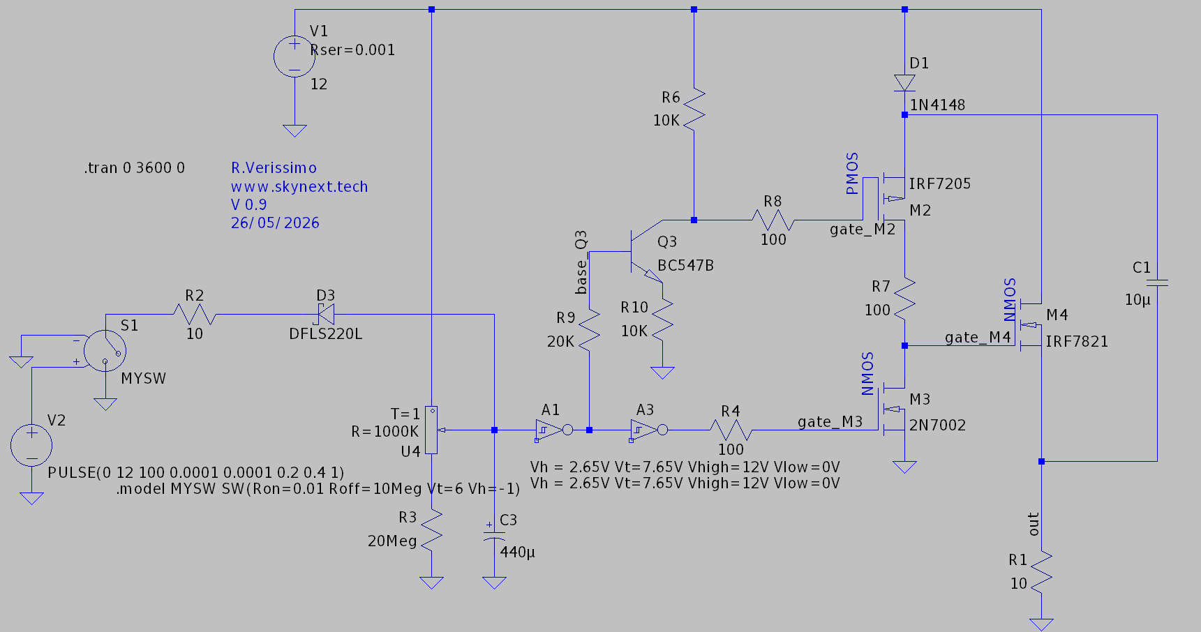
When it comes to switching timer modules, most designs are either based on the good old 555 timer, or some kind of 8 bit MCU that performs supervisory functions (like turning a relay off and keeping track of time), with the advantage for the later to allow for various timing and delay on/off programs. Most designs however, draw hundreds of microamperes up to several milliamperes while idling. Since one common use of these timers is to power a load for a given time in off grids setups where stored battery energy must be conserved, a low quiescent current solution would be a preferable design. Most designs are also relay based. Sturdy relays have an advantage of providing NC/NO modes natively, tolerate inductive kickback from loads such as motors, and are immune to spurious turn-ons.
Here we present a fully solid state timer delay off high side NMOS switch, thus with low Rds ON. The power to the load is turned on through a pulse (such as one supplied by a spring loaded pushbutton), latches, and turns off based on the timing constant of a RC network.
Giving the maximum rating of the CD40106 Schmitt trigger used here, the maximum switched voltage is around 18V. A higher voltage rated Schmitt trigger inverter would allow 24V operation, and using MOSFET rated above Vds of 30V would push operation voltages into 48V or more.
Download
Operation.
The transient connection of the switch S1 discharges the capacitor C3 through D3 to ground, bringing temporarily the schmitt trigger input to ground potential. output of the trigger goes to logic 0V, while the inverting input goes to logic high. A CD40106 schmitt trigger can be used to implement complementary outputs, by daisy chaining two stages as shown in the schematic (A1 and A3). The operational parameters of the CD40106 at 12V have been calculated from the datasheet and added to the model.
In the low voltage state, the first inverting output of the schmitt trigger A1 is in logic high, sinking current into Q3 base, which has the effect to lower gate potential of PMOS M2, turning it on, and supplying bootstrap capacitor voltage to M4, which turns it on and performs the intended high side switching function, While schmitt trigger A3 output voltage goes 0V, turning M3 firmly off and preventing fast discharge of C1.
When the RC network charges back above Vhigh threshold, M2 is turned off, which has the effect of stopping the supply of voltage from the bootstrap capacitor to M4, and bringing the gate of M4 to ground through the turn on of M3. This effectively turns off M4.
Giving the low gate charge and leak of modern NMOS, the bootstrap capacitor C1 can supply voltage to the gate of M4 over a time far longer than the time constant of the RC network made with U4 + R3 and C3.
Note that M2 does not handle large currents in that circuit. A smaller footprint PMOS could be used, rated for logic Vgs levels (such as -5V)
Note that the transition Vhigh and Vlow voltage of the CD40106 used are linear functions of supply voltage, Which means that a higher or lower Vcc operation as supplied from a battery should not change the minimum and maximum delays achieveable significantly.
Resistor R7 acts as a current limiting resistor for gate current but also during switching of M2 and M3, which could temporarily provide a low impedance path to ground. Note that CD40106 propagation delay using two stages in a daisy chain have the effect of introducing a small dead time between M2 and M3 switching, thus mitigating that unwanted effect.

Leave a Reply