Category Studies and Reports

Analog Devices AD7606-8 on Raspberry pi zero W

Abstract :

This article documents the development and testing of the Linux driver module and the interface between the Raspberry Pi GPIOs and the AD7606-F4 development board. The AD7606-F4 is based on the AD7606-8, The 8 channel version of the AD7606, true bipolar, ±5V / ±10V input range, 16 bit, with 1 to 64 hardware oversampling, simultaneous sampling ADC. The driver development effort is focused on the 16 bit parallel interface mode instead of SPI. It leverages the Linux industrial IO layer. The goal is mainly to characterize maximum achievable sample rate / triggering rate, as well as sample loss and jitter induced by kernel burden and scheduling, depending on triggering rate, while using “worst case” interfacing. No backend IC is used to perform hardware protocol management and hardware buffering in our tests.

Using a small SOC with limited RAM and CPU capabilities also conforms with worst case performance testing, and will allow us to identify the limiting factor of such a setup.

Initial driver development was performed by Analog Devices and the driver maintainer and is available in the linux kernel source. It lacked however several features, but offered a good starting base for a fully functional driver. The available driver is split into two source files, one for the parallel interface and one for the SPI interface.

We will explore the various methods of interacting with GPIOs inside the kernel module, as to improve the conversion/read cycle time for all channels.

The maximum sampling speed is mainly dictated by the kernel load, as a direct interfacing of the AD7606 to the Raspberry Pi requires handling interrupts at the sampling speed. The main limiting factor however seems to be the gpiod_set_raw_value() execution time, and thread synchronization between the trigger handler and the IRQ handling callback, limiting sampling rate short of 8 ksps.

IIO provides a mechanism, called backend, to interface signaling (such as conversion start, handling of IRQ and first channel read detection) by an intermediary device such as an IP core. This provides also hardware buffering so that IIO gets data from the hardware buffer in chunks, so that IRQ loading to the kernel is lowered.

Note that besides kernel performance limitations, high sampling rates also require application of common hardware interfacing best practices, such as :

  • Minimising trace or cable length to minimize loop inductance
  • Keeping same trace length, but it is secondary since the baud rate is still conservative even at the max rate allowed by the ad7606, dicated by the minimum timings specified in the datasheet.
  • Adding small values resistors such as 51 ohm on the lines to minimize ringing
  • Adding guard traces grounded on one side to reduce crosstalk and inductive coupling between data lines, and between signalling lines.
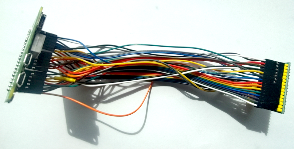
  • The GPIO pin layout vs the line pin layout on the AD7606-F4 dev board we are using cannot allow the use of a 40 pin ribbon cable such as those use for ATA UDMA transfer, as it would require crossing over lines, so a mating PCB or hat design is required.
  • Low sampling rates can be achieved using standard dupont cables, and assessing the sampling rate limits for such a solution is one of the goals of this article.

Note that using 20cm dupont pin cables, without current/ringing limiting resistors as inductive dampers, it is highly improbable to reach sampling rates such as 48 ksps as found on audio interfaces using backend-less interfacing. Pushing the sampling rate above 8 ksps would mainly require, in that order :

  • MMIO for signalling (CONVST, CS/RD strobes) instead of reliance on gpiod_set_raw_value()
  • Using try_wait_for_completion() in a preempt_disable() / preempt_enable() context
  • A more robust and faster SOC, with dual core at least to enable IRQ pinning on a core
  • Using a RT linux kernel
  • A hat or PCB mating interface to improve signal integrity

However, determining the practical limit of such a solution is useful as it is the most cost effective and fast way to interface a Raspberry Pi or other SOC to perform ADC operations using the industrial IO layer.

The Github link to the kernel module driver and its associated helpers is available at the very end of this article.

General interfacing using the parallel interface layer.

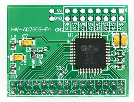
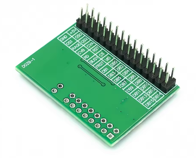
The AD-7606-F4 development board we used and available on Aliexpress or other chinese marketplaces has a small footprint. The development board we got does not exposes the standby pin, and was factory set for parallel interface transfer through a SMD resistor on the 8080 pad identified by silkscreen marking. Swapping the resistor into the SPI pad would obviously enable SPI mode. Note that the AD7606, to achieve full sampling rate performance for SPI requires dual SPI mode.

In parallel mode, the signalling requires at least the following lines connected between the AD7606 and the Raspberry Pi :

We will use the Raspberry Pi (host interface, as the reference for IN/OUT specification)

  • CONVSTA/CONVSTB : these two lines can be tied together into a single GPIO on the Raspberry Pi. These are OUT pins. They are strobed low to signal that we want to initiate a conversion. if the pins are strobed low at the same time, all 8 channels are simultaneously sampled, if strobed independently, they allow sampling of the first 4 and last 4 channels independently, the sampling delay allows compensation of group delays induced by filters or CT vs VT in power grid measurements.
  • BUSY : IN pin, the falling edge indicates end of conversion and signals the SOC (through GPIO IRQ management) that it is ready for data reading of all channels.
  • FRSTDATA : IN pin, this signals the readout of the first channel, so that there are no channel alignment issues : if FRSTDATA level is not high when the SOC reads the first channel as the driver internal state indicates, or if FRSTDATA level is high when the SOC expects to read subsequent channels, it should be treated as an IO error and all channels samples should be discarded from the read cycle. The AD7606 should be reset through the RESET pin. Monitoring RESET events from this condition is recommended in the debugging phase, as it indicates potential hardware interfacing problems and instability. If too much FRSTDATA mismatches occur, try increasing timing delays for all pin strobes.
  • RESET : OUT pin, commands the AD7606 to reset. Used if an inconsistent state is detected, see above. A reset event will lower sampling rate, as the interface needs some time after the reset to be fully operational. Reset is also called in the probe function at device initialization as the ad7606 should be reset after power-up or resume from standby.
  • CS/RD : OUT pins. tells the AD7606 to shift next channel into the parallel interface registers, and select the AD7606 if they are stacked on the same parallel line. if exactly one AD7606 is present on all lines, then CS/RD can be strobed simultaneously (linked mode). Signaling is easier this way, as independent CS/RD management gives a slightly different timing protocol. Refer to the datasheet for independent management of CS/RD. Our driver uses linked CS/RD mode, but our tests were performed with two separate lines driven concomitantly. (GPIO levels set on two pins synchronously)

The remaining pins, RANGE, 0S0, 0S1, 0S2 are configuration pins used to select the input voltage range specification (+-5V or +-10V) and OSx pins are used to set the bits that select the oversampling mode.

The AD7606-F4 dev board does not expose the STBY pin on the 40 pin header.

The “VO” pin on the AD7606-F4 corresponds to the AD7606 Datasheet pin mnemonic “VDRIVE“. This pin should be connected to the 3.3V line of the Raspberry Pi. This line supplies the logic power and sets the levels used on the data pins, FRSTDATA, and BUSY.

In our setup, leftover pins are GPIO0, GPIO1 and GPIO27. GPIO0 and GPIO1 are reserved and used by external EEPROM hats, they can be reclaimed using the force_eeprom_read=0. This prevents EEPROM boot time operations on these pins. We did not test these pins in our use case. GPIO27 is leftover.

If CS/RD were tied, another pin would be returned to the pool of free pins, making 4 leftover pins.

Oversampling can be configured statically to reclaim 3 more pins

In order to avoid interface conflicts, raspi-config or edition of /boot/firmware/config.txt should be performed to disable pin functions such as UART, SPI, I2C, 2wire, EEPROM.

Parallel interface Data Pins

The AD7606 provides byte mode parallel transfers besides word parallel mode, in byte mode, each channel data is supplied to the host through two successive data reads. (MSB/LSB or LSB/MSB). This mode halves the maximum achievable data rate, but allow recovery of 8 pins for other uses.

The 16 bit (word) data transfer rate, require a single CS/RD or RD strobe per channel read, at the expense of using a full 16 pin block. This is the mode we used in our demo.

Note that data line pin mapping between the host and AD7606 should be contiguous and ordered to prevent unnecessary bit reordering and masking. GPIO order is determined by the BCM GPIO pin nomenclature, not pin ID number.

Bit shifting is required however if the data lines start at an offset, that is, if they don’t start at GPIO0.

In our use case, we used the GPIO8 to GPIO23 range as the 16 parallel GPIO lines. ARM architecture is optimized to read 32 bits, with correct alignment when using MMIO (memory mapped IO), which means, in our case, reading 4 bytes at GPIOLEV0 offset, and extracting the 2 center bytes, which requires a simple bit shift, bit mask and cast to u16 operation. for MMIO, we used the industry tested readl() MMIO function, although recent kernel practices seem to shift towards the use of ioread32(), Which seems to work well too in our tests.

MMIO in kernel space on the Raspberry Pi Zero W.

Using gpiod_get_* functions for parallel data transfers is grossly inefficient. That is why a more direct path is required for transfers, which is achievable using memory mapped IO. This will be tested in future revisions of this article.

Basically, performing MMIO requires knowing the Physical memory mapping base address of the BCM8235 bus address. On Raspberry pi Zero W, it is 0x20200000. (not 0x7…, as indicated as base on the BCM8235/6 datasheet : this is the BUS address, and not 0x32…. : this is the physical memory mapping on newer Raspberry pi Boards such as Pi2/3/4)

Note that the pinctrl tool can be used to ascertain the physical memory mapping base address. Here is the trap however : 0x32000000 base address seems to work in our case to get GPIO levels using a mmap wrapper with Python, since it reflected pin changes, but it did not work in kernel space, so this address base is misleading.

However, The correct 0x202000000 physical memory address base cannot be accessed directly in kernel or user space though. It needs another remapping operation into kernel virtual memory address space.

This is where the request_memory_region() and ioremap() functions come into play and shall be used in the kernel driver module.

request_memory_region() reserves the physical memory region for ioremap(), and prevents any outside access from kernel or user space, which could lead to instabilities and conflicts. Once the requested memory region is allocated to the kernel module drive through the former call, any other request, read or remap operation will result in an error, such as EBUSY.

This is also why disabling conflicting functions such as I2C, SPI, UART, 2wire, EEPROM and consorts that would conflict with the module is required

In our case, we disabled all of the above mentioned functions.

Device Tree Overlays

The driver needs to know which pins to use and which MMIO address space to use. The current best practice is to use only device tree overlays that provide platform specific and implementation specific GPIO pin mapping and MMIO base address information. Using .c or header files as driver board configuration files is a deprecated and discouraged practice, especially in loadable/unloadable (not kernel integrated) modules.

This is why writing a device tree (dts file) overlay is mandatory.

The device tree provides signalling and configuration pin information, as well as data lines pins declaration. The signalling and configuration pin information is used by GPIOd_* functions.

Although data line pins are used by MMIO, which does not use GPIOd_* functions for data transfer, the pin declarations as an array of pins in the device tree overlay is required for configuration of these data line pins as INPUTS, which is done once in the module .probe() callback function, and this step uses GPIOd_set functions for mode configuration.

Configuration of the physical base address used to access GPIOLEV0 registers and data transfer, so that request_mem_region() and ioremap() get the required base address information and number of memory pages to remap is done through the “reg” device tree property.

reg = <0x20200000 0x00004096>;

the first hexadecimal number is the physical memory base address of the GPIO peripheral, and the second number is the number of bytes to be used in request_mem_region() and ioremap() functions.

Note that ARM paging requires at least 4 bytes as size, in our case we mapped a full SZ_4K region, at it is usually done in other similar drivers. The start address needs to be aligned at 4 bytes, which is the case as it is divisible by 4. The total GPIO address space is x bytes.

the “adi,” prefix encountered in properties can be seen as a namespace information (Analog Devices manufacturer), and is used to avoid ambiguous / property name conflicts with other existing device tree properties at the time of dtoverlay loading. This is preferable since some common tokens such as ‘reset’ may already be used.

Pull up / Pull down configuration

Standard pin definitions <&gpio pin_number flags> as pin desc definitions used by the ad7606 are not sufficient to specify the configuration of the internal pulls. These need to be specified as the brcm2835 device level, and referenced by the ad7606 device tree fragment. Pull ups / Pull down not only allow the logic state to settle if the driving side is in high-z mode such as the tri-state FRSTDATA pin, preventing undefined behaviour, they also allow quicker rise and fall edge timings, which is a requirement for high speed transfers.

/dts-v1/;
/plugin/;

#include <dt-bindings/gpio/gpio.h>
#include <dt-bindings/interrupt-controller/irq.h>

/ {
    compatible = "brcm,bcm2835";
    fragment@0{
        target = <&gpio>;
        __overlay__{
                frstdatapin: frstdatapin {
                    brcm,pins = <7>;
                    brcm,function = <0>;
                    brcm,pull = <1>; 
            };
                busypin: busypin {
                    brcm,pins = <4>;
                    brcm,function = <0>;
                    brcm,pull = <1>; 
            };
                parallel_datapins: parallel_datapins {
                    brcm,pins = <8 9 10 11 12 13 14 15 16 17 18 19 20 21 22 23>;
                    brcm,function = <0 0 0 0 0 0 0 0 0 0 0 0 0 0 0 0>;
                    brcm,pull = <1 1 1 1 1 1 1 1 1 1 1 1 1 1 1 1>; 
            };


        };    
    };
};


/ {
    compatible = "brcm,bcm2835";
    fragment@1{
        target-path = "/";
        __overlay__{
        #address-cells = <1>;
	    #size-cells = <1>;
	    ad7606-8@0 {
                compatible = "adi,ad7606-8";
                reg = <0x20200000 0x00004096>;
                avcc-supply = <&vdd_5v0_reg>;
                interrupts = <4 IRQ_TYPE_EDGE_FALLING>; /* linked to AD7606 busy line ? */
                interrupt-parent = <&gpio>;
                adi,conversion-start-gpios = <&gpio 5 GPIO_ACTIVE_HIGH>;
                reset-gpios = <&gpio 6 GPIO_ACTIVE_HIGH>;
                adi,first-data-gpios = <&gpio 1 GPIO_ACTIVE_HIGH>;
                cs-gpios = <&gpio 2 GPIO_ACTIVE_HIGH>;
                rd-gpios = <&gpio 3 GPIO_ACTIVE_HIGH>;
                cs-rd-gpios = <
                &gpio 2 GPIO_ACTIVE_HIGH 
                &gpio 3 GPIO_ACTIVE_HIGH
                >; 
                adi,oversampling-ratio-gpios = <&gpio 24 GPIO_ACTIVE_HIGH
                                &gpio 25 GPIO_ACTIVE_HIGH
                                &gpio 26 GPIO_ACTIVE_HIGH>;
                standby-gpios = <&gpio 27 GPIO_ACTIVE_LOW>;
                adi,parallel-data-gpios = <
                &gpio 8 GPIO_ACTIVE_HIGH
                &gpio 9 GPIO_ACTIVE_HIGH
                &gpio 10 GPIO_ACTIVE_HIGH
                &gpio 11 GPIO_ACTIVE_HIGH
                &gpio 12 GPIO_ACTIVE_HIGH
                &gpio 13 GPIO_ACTIVE_HIGH
                &gpio 14 GPIO_ACTIVE_HIGH
                &gpio 15 GPIO_ACTIVE_HIGH
                &gpio 16 GPIO_ACTIVE_HIGH
                &gpio 17 GPIO_ACTIVE_HIGH
                &gpio 18 GPIO_ACTIVE_HIGH
                &gpio 19 GPIO_ACTIVE_HIGH
                &gpio 20 GPIO_ACTIVE_HIGH
                &gpio 21 GPIO_ACTIVE_HIGH
                &gpio 22 GPIO_ACTIVE_HIGH
                &gpio 23 GPIO_ACTIVE_HIGH
                >;
                adi,sw-mode;
                status = "okay";

                pinctrl-names = "default";
                pinctrl-0 = <&frstdatapin &busypin &parallel_datapins>;
            };
        };
    };
};

Makefile information

The Makefile is used to compile two units :

  • The device tree, with a preprocessing step. the dts files get pre-processed into a dts.preprocessed file, which itself gets compiled into a binary device tree object (dtbo) that can be used by device tree overlay loading functions such as dtoverlay or dtoverlay statements in the Raspberry Pi /boot/firmware/config.txt
  • The driver itself, made from one c file and one header files (ad7606_par.c and ad7606.h)
obj-m +=ad7606_par.o
CFLAGS_ad7606_par.o := -UDEBUG
EXTRA_CFLAGS += -fno-inline

all: module dt
	echo Built Device Tree Overlay and kernel module

module:
	make -C /lib/modules/$(shell uname -r)/build M=$(PWD) V=1  modules
dt: ad7606.dts
	cpp -nostdinc -I /usr/src/linux-headers-$(shell uname -r | sed 's/-rpi-v[0-9]*//')-common-rpi/include/ -I arm64  -undef -x assembler-with-cpp  ad7606.dts ad7606.dts.preprocessed
	dtc -@ -Hepapr -I dts -O dtb -o ad7606.dtbo ad7606.dts.preprocessed

clean: 
	make -C /lib/modules/$(shell uname -r)/build M=$(PWD) V=1 clean
	rm -rf ad7606.dtbo ad7606.dts.preprocessed

Module Loading helper bash script

The file load.sh is used as helper to load the device tree and kernel driver, as well as its dependencies. In a final driver and its installation procedure, the dependencies are usually stored as lines in a dependency file, .dep.

At the time of writing this article, distribution effort was not yet done, and so it is outside the scope of the article. Which means that modprobe calls in the correct order have to be done to load the required dependencies.

Those are :

  • industrialio
  • iio-trig-hrtimer
  • industrialio_triggered_buffer

Then, the hrtimer0 instance is created as it will be subject to validation by our driver module validate trigger function.

following is the DT overlay load and the kernel module load. The remaining calls are used to configure the sample buffer, triggered buffer sampling frequency (managed by iio hrtimer), and buffer enable at the end, with a real time read of the iio device by using dd.

Commented calls are used for ftrace profiling, to minimize dev_dbg overhead.

#!/bin/bash
sudo modprobe industrialio # load industrial io kernel module
sudo modprobe iio-trig-hrtimer # load hrtimer industrial io kernel module
sudo modprobe industrialio_triggered_buffer # load industrial triggered buffer kernel module
sudo mkdir /sys/kernel/config/iio/triggers/hrtimer/hrtimer0 # configure one hrtimer instance
sudo dtoverlay -v ad7606.dtbo #load compiled device tree snippet with ad7606 pin to rpi config
sudo insmod  ad7606_par.ko #load ad7606 driver module
sudo sh -c "echo 10.0 > /sys/bus/iio/devices/trigger0/sampling_frequency" #sets triggered sampling frequency to 10 sps
sudo sh -c "cat /sys/bus/iio/devices/trigger0/name > /sys/bus/iio/devices/iio\:device0/trigger/current_trigger" # configure the ad7606 iio device to use the hrtimer0 instance
sudo sh -c "echo 1 > /sys/bus/iio/devices/iio\:device0/scan_elements/in_voltage1_en" # configure the triggered buffer to output a single channel, the second channel. (channels are 0 indexed)
cat /sys/bus/iio/devices/iio\:device0/in_voltage1_raw #output raw value for testing. The first sample is usually invalid, this needs debugging.
cat /sys/bus/iio/devices/iio\:device0/in_voltage1_raw #gets another sample, this value should be ok.
#sudo vclog -m


#Make sure tracing is disabled during tracing reconfiguration
#echo "disabling tracing and current_tracer"
#sudo sh -c "echo 0 > /sys/kernel/debug/tracing/tracing_on"
#sudo sh -c "echo nop > /sys/kernel/debug/tracing/current_tracer"


#sudo sh -c "echo ad7606_* > /sys/kernel/debug/tracing/set_ftrace_filter"
#echo "ad7606_* written to set_ftrace_filter"
#sudo sh -c "echo function_graph > /sys/kernel/debug/tracing/current_tracer"
#sudo sh -c "echo 2 > /sys/kernel/debug/tracing/max_graph_depth"
#echo "set max_graph_depth to 2"

#sudo sh -c "echo 1 > /sys/kernel/debug/tracing/tracing_on"
#echo "function_graph enabled in current_tracer, and enabling tracing "

echo "now enabling device buffer"
sudo sh -c 'echo 1 > /sys/bus/iio/devices/iio\:device0/buffer0/enable'
echo "buffer enabled"

#echo "reading trace_pipe in 2 secs"
#sleep 2
#sudo sh -c "cat /sys/kernel/debug/tracing/trace_pipe > /root/trace.log"

echo "will now output raw, aligned sample bytes from buffer device"
sudo sh -c "dd if=/dev/iio\:device0 bs=20 iflag=fullblock | hexdump"

Performance testing

The following picture shows the testing conditions. Such a crude interface is useful for getting “worst case performance” data, which are useful in setups where the AD7606 must be up and running in the least amount of time and least amount of money (from placing order to sampling, using off the shelf components)

When using MMIO for data transfer, and gpiod_* functions for signalling CONVSTx, CS/RD, and reading FRSTDATA, the gpio_d* function calls will be bottleneck. A full convst/read cycle takes around 60us. In that case, the maximum theoretical sampling rate would be 15 ksps. We expect that 8 ksps could be a conservative max practical limit accounting for kernel IRQ burden. Using full MMIO would probably help push the limit higher, if care is given to disable as much system noise as possible (such as HDMI, videocore drivers, bluetooth, framebuffers, etc). A more capable raspberry pi such as 3/4 which have more than 1 core, could use IRQ pinning to help such a fully MMIO optimized driver to work at maximum speed, provided a mating board or a full fledged ad7606 hat is used for hardware performance.

The FRSTDATA channel synchronization mechanism and error rate

The tristate (High-Z, HIGH/LOW) FRSTDATA input is used to signal that the first channel is ready to be read. This hardens the transfer protocol as the sample frames remains aligned, that is, the channels do not get misaligned in the output buffer. Algorithmically, a boolean “first-channel” is set to true at the beginning of the samples read process. it is compared to the level of the FRSTDATA pin, and the comparison should branch to true. The boolean is then set to false and compared to FRSTDATA level for the remaining channels and should also branch to true. If there is a mismatch, sample readout is aborted, and a RESET is sent to the ad7606, through the ad7606_reset functions, and the that were abl where the internal driver pin state is also reset so that the whole conversion/readout cycle can be resumed.

The FRSTDATA pin is a good indicator of hardware stability and hardware interfacing quality. Lowering strobe cycle periods and overall timing delays will typically increase the number of spurious FRSTDATA states and subsequent resets, especially when reaching the limits of hardware interface stability, which can happen well before the timing limits of ad7606 datasheet when using an ad-hoc long Dupont header pins cable interface. In our case, the IRQ load on the kernel as well as the gpiod_set_* command timing overhead are the bottleneck.

For reference, This is the average spurious FRSTDATA error rate over 1 hour sampling at various sampling rates. Test conditions : Raspberry Pi Zero W, 20 cm Dupont header cables, internal pulls used on all input pins, no current limiting resistors.

1000 sps = 2.44 %

2000 sps = 2.74 %

4000 sps = 3.08 %

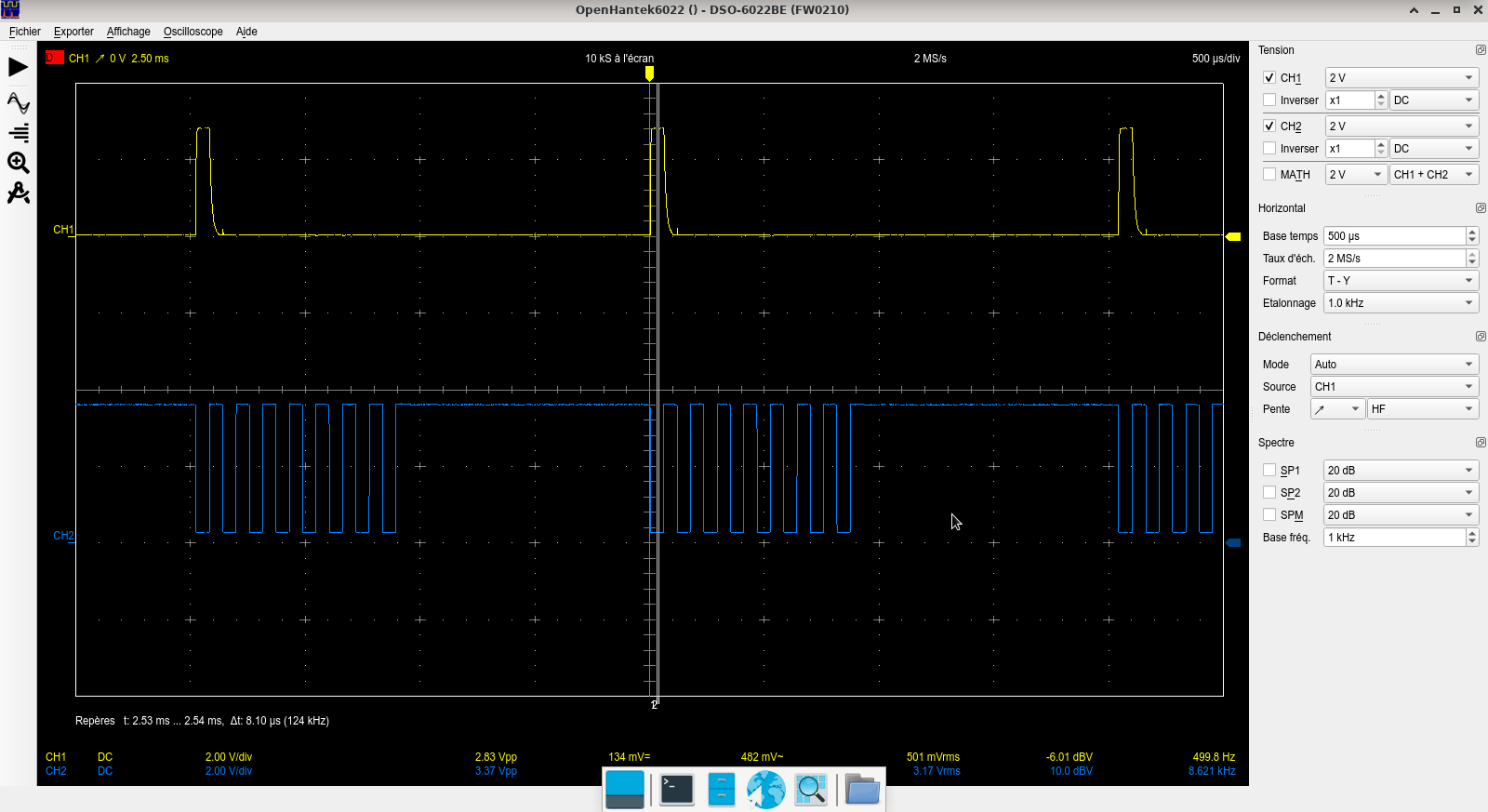
The following oscilloscope capture shows the FRSTDATA channel read synchronization signal on CH1 and the linked mode CS/RD pulse strobes used to latch all channels (8) data into the parallel interface lines

FRSTDATA (CH1) and CS/RD (CH2)

timer trigger callback function performance

We tested three code combinations to jauge performance

  1. gpiod_set_raw_value() functions for CONVST and CS/RD strobes + wait_for_completion_timeout() synchronization.
  2. MMIO based CONVST and CS/RD strobes + try_wait_for_completion() after usleep_range(5,10)
  3. MMIO based CONVST and CS/RD strobes + wait_for_completion_timeout()

at a sampling rate of 100sps, with an incompressible strobe time of 200ns.

The run time of the callback , averaged over 500 trigger calls are

(1) = 122 µs

(2) = 108 µs

(3) = 100 µs

In our case the best execution time of the trigger handler was on average 100us, using 100ns timing for pin strobe delays. Note however, that most of the time spent is not accounted from these timing delays, but by the slowness of the gpiod_set_* functions, MMIO write to a lesser degree, buffer publishing to the IIO stack and IRQ thread synchronization to trigger handler using completions. The CONVSTA/B to BUSY falling edge published in the datasheet is specified as 5us, which is a minor contribution to the overall cycle. Note that wait_for_completion_timeout() puts the thread on the wait queue, and the IRQ handles completion using complete(), which resumes the trigger handler thread, this has probably quite some overhead, but is safe in IRQ contexts, It seems however that for a 5 µs conversion time, there is no performance gain, but loss, using the usleep_range(5,10) + try_wait_for_completion() combination. Using MMIO gives a moderate performance boost. Overall the limiting factor seems to be MMIO performance and iio_push_to_buffers_with_timestamp() performance, which could improve with faster cores and memory. Compared to older buses such as PIO ATA (Programmed IO mode, that does not leverage DMA) the maximum throughput would be 8 * 2 bytes / 100 µs = 160 kB/s, which is still 20 times slower than PIO Mode 0. Thus continuing effort on investigating MMIO performance and IIO call responsivity is required, as several studies have shown, with oscilloscope proof, that Mhz frequency range strobes are possible on Rpi, albeit using tight loops MMIO strobes. A further investigation on each code component contribution inside the callback would allow a precise evaluation of performance, and using an oscilloscope instead of relying on kernel timestamp tracing, which have a non negligible overhead.

wait_for_completion_timeout() also returns a non zero integer if timeout is not reached, representing the remaining jiffies in the supplied timeout. It can thus be used to check the time waited by a simple subtraction. Note that with a kernel “HZ” value of 100, one jiffy is 10 msec, which resolution is too low to provide any sensible performance metric for tuning. Any value returned different of the supplied timeout would only inform of a severe contention of IRQ mishandling.

At 100 us conversion/read cycle, the theoretical maximum sampling rate is short of 10 ksps.

Maximum toggling speed using MMIO in tight loop

As noted in (1), the maximum toggling speed on Raspberry Pi 1 (using a preformatted 32 bits mask) “Direct output loop to GPIO” was stated to be 22.7 Mhz, backed by oscilloscope readings.

It looks like the code was ran from user space using /dev/mem mapping.

We managed to get a speed of 24.9 Mhz from kernel space, using the boot config CPU boost (overclock) and a proper heatsink. Although it is not backed from oscilloscope reading to reflect waveform quality yet, though the following code, using the GPIO “standby” pin in our module, as it is not used by the AD7606-F4 development board.

#define MMIOTEST(x) x ? iowrite32(standbybit,st->base_address_set) : iowrite32(standbybit,st->base_address_clr);


void ad7606_pin_benchmark(struct ad7606_state *st)
{

	u32 count = 1000000;

	struct timespec64 ts1;
	struct timespec64 ts2;
	
	ktime_get_ts64(&ts1);

	while(count)
	{
		MMIOTEST(0);
		MMIOTEST(1);
		count--;
	}

	ktime_get_ts64(&ts2);

	struct timespec64 ts3 = timespec_subtract(&ts2,&ts1);
	dev_info(st->dev,"ad7606_pin_benchmark, 1e6 pin strobes, time taken:[%5lld.%06ld]\n",(s64) ts3.tv_sec,ts3.tv_nsec/1000);
	
}
[ 1292.127770] ad7606 20200000.ad7606-8: ad7606_pin_benchmark, 1e6 pin strobes, time taken:[    0.040128]

Github repository of kernel module driver code and helpers

https://github.com/rodv92/ad7606_par_rpi

Moving forward

While this approach can get you sampling 8 channels fast, it mainly limits to slow sampling requirements and cannot guarantee equispaced sampling. On the other hand, no hardware buffering means the latency is minimal, and it also builds on top of IIO seamlessly.

For serious speeds a fully integrated acquisition system featuring a MCU and the AD7606, and a convenient interface such as USB is preferable.

An AD7606 development board is 7 to 11 USD pu (Aug 2025).

A full-fledged USB acquisition system based on AD7606 is expected to cost 50 to 60 USD p.u. (Aug 2025).

Such a system will probably be the focus of our interest in our next article about the AD7606. Stay tuned.

2025 R&D Strategy forecast and 2024 Annual report.

Section I – R&D strategy forecast

Our Research on 2025 will focus on metering devices tailored for emerging markets. Specifically, our goal is to provide a portable, computer driven phasor measurement unit and power quality analysis solution for Low/Medium voltage (110V-230V to 11kV) at a fraction of the price tag of market leader solutions, which would leverage existing DAC solutions, such as professional USB sound cards instead of costly DAQ platforms or integrated solutions. Most of the R&D effort will be focused towards PC software development. A calibration channel will be provided to take into account hardware induced frequency and phase response variation as well as vendor specific sound cards delays, as well as audio interface (ASIO,Directplay, etc.) delays.

As for financing, we plan to introduce a comprehensive crowdfunding program. We also envision a crowdsourcing initiative for engineers that wish to contribute to this endeavour. This will help in kick starting the project and ensure viable time to market delays. Stay tuned.

A significant part of the project is already underway. We do not start from scratch at the present.

The final implementation will be IEEE Std C37.118.1 compliant.

Section II – 2024 Annual report

2024 Annual report will be made available January 2nd, 2025.

Ltspice synchronous generator model in abc reference frame coupled with VAWT prime mover and DC battery charging load.

Simulation model

April 2025 Update!
1SYNC_GEN_v2 model now uses more realistic inductances and field winding resistances, and rotor moment of inertia (assuming a 30 kVA generator model)
Better initial convergence and faster simulation.
Field excitation is now current source driven as it should be.
Ratio of field excitation energy expenditure to net electrical power closer to 1% (as it should be)
We also tested with relaxed SPICE engine “tol” parameters down to 2 orders of magnitude, and the model simulation is numerically stable. This increases simulation speed.
Added also in the download archive a generator model with a simple P/I control voltage (AVR) and frequency. not optimized.
Updated model only contains core generator, fault testing and rectifier have been taken out for faster simulation. We will update the full model and VAWT soon.

LTspice tweaks for tolerance parameters lowered some orders of magnitude for simulation speedup.
Generator start with excitation soft-start from 0 to 10A from 0 to 1 second.
Excitation power (top chart) to net electrical power (second from top) ratio is close to the 1% expected. Second and third chart dimension is kW, not KV, fourth is RPM, (units are not properly displayed as the chart data comes from the output of a behavioural voltage source that is solely used as a display helper.)

Previous models :

Two simulation models are provided :

VAWT_generator_and_crowbar.asc : Provides the VAWT generator model and synchronous generator with excitation winding, rectifier, and crowbar circuit.

VAWT_generator_and_PWM_charger.asc : Provides the VAWT generaor model and synchronous generator wih excitation winding, rectifier, and crude PWM charger. (for 48V battery bank).

Limitations are mainly due to the simulation speed restrictions.

Requires Ltspice 17.1 or newer. May require some component models, such as for specific MOSFETS.

Incentive.

The following work proposes an exploration of behaviour of medium size residential/agro/community wind turbines when coupled to a synchronous generator with field excitation.

Traditionnally, small synchronous generators with field excitation are usually found in small hydroelectric generation setups.

While most commercial devices in the wing generation category are fitted with PMSM (Permanent Magnet Synchronous Generators).

PMSM usually present lower inertia, include rare earth material magnets which contribute significantly to the overall cost of the generator, and which cost is expected to grow significantly due to undersupply and large demand for the EV market.

https://www.mining.com/supply-of-rare-earth-magnets-wont-keep-with-demand-by-2040-report/

Permanent Magnets are desirable for small to medium power sizes due to the absence of field losses, which contribute substantially to the total power loss of the generator for small scales, Beside magnets most PMSM rotor configuration use electrical steel to form either salient or round rotors. The main difference from an economical perspective is cost of copper or aluminum vs rare earth magnets as initial cost, and lower efficiency due to field excitation as a variable and recurring loss. These range in the 2% to 4% for operation at nominal conditions for a 75kVA machine. Our investigation will assume first a constant excitation, variable voltage operation, While control of excitation will be considered for dump load operation (braking) on a static resistive load, with the intent of thermal generation in high wind power conditions. Also, we will take into account the stalling speed of the VAWT and update the control law accordingly to prevent this phenomenon. We will also investigate alternative control laws for dump load operation and braking, under constant field and variable output impedance (simulating a servo-rheostat load). These are mainly of use for PMSM dump load operation (whose field is constant)

Synchronous Generator model part.

The model represents a synchronous machine with the following characteristics :

3 phase stator, wye configuration.

Variable field excitation, though the model does not implement AVR based on excitation control, at least for now. Variable field excitation is investigated for dump load (crowbar) operation.

Note that permanent magnet synchronous generator could be crudely modelled by this instance by setting an adequate static field strength (with no ramp up) and by setting a higher number of poles. Note that most PMSG designs do not use dampers.

Parametric number of poles. Note also that q-damper winding inductance is valid for a two pole machine, for p > 2, q-damper self and mutual inductances should be set to 0. (or the q-damper excluded from the circuit)

Rotor Saliency is modelled, through the Lms parameter.

Model is based on flux linkages. It specifies leakage, mutual inductance, and resistance of each winding. The model is ‘lumped’ in terms of inductances, i.e. it does not specify inductances as a function of winding geometry (number of turns, area, length, permeability.. etc.)

All mutual inductances are modelled (stator phase to each other stator phase, rotor field to each rotor damper, and stator phase to each rotor winding)

The default setup includes one damper coil on the d axis and one damper coil on the q axis, and uses a two pole rotor by default.

This makes 6 flux expressions with 6 components each : 1 flux component arising from self inductance, and 5 components corresponding to mutual inductances since there are 6 windings in total.

Due to a quirk in the Ltspice parser for arbitrary inductors based on flux expressions, I had to separate self flux from the mutual flux expressions.

Ltspice expects the current flowing through the inductor to be represented by the variable ‘x’. Thus I had to use the form Flux = Lself*x + sum(flux_linkages)

That is why the flux linkages expressions in the following screenshots have 5 components instead of 6. the final flux expression combining them all is specified in the inductor ‘Flux=’ expression, seen in Figure 5.

Figure 1 Natural inductances parameters
Figure 2 Stator self inductances expressions
Figure 3 Stator flux linkages expressions
Figure 4 Rotor flux linkages expressions
Figure 5 Stator equivalent circuit
Figure 6 Rotor equivalent circuits

Magnetic saturation effects are not modelled for now. Usually the field winding is driven close to saturation, which makes this modelling significant, at least for large generators.

Space Flux distribution does not model anistropies coming from the rotor shoe and stator wedges and slots physical geometry. These flux anisotropies give rise to EMF with harmonic distortion. It only models those coming from the saliency model, which is a first order approximation.

The model uses the LTspice arbitrary inductor model to express self flux and flux linkages. The windings thus use inductors as the source of emf, not behavioural voltage sources. The only inductor that is powered by a DC source is the field winding.

The main incentive of using abc frame equivalent circuit instead of a faster dq0 reference is that :

A model in abc reference frame has the advantage of being better suited for non steady state, non linear loads, islanded mode (not connected to the grid).

As an example, the model feeds a resistive load and smoothing capacitor through a 6 diode three phase passive rectifier. Despite the load non linearity, the model performs well.

The model does not drive the shaft at synchronous speed (steady state turns/min shaft rotational speed provided by the manufacturer), it takes as an input mechanical power from the VAWT, which itself is a function of wind speed (provided through the V12 source PWL input) and VAWT rotor speed. A steady mechanical input power, modelled through the V2 source, can be swapped instead of the VAWT for debugging purposes.

A further refinement of the model for MPPT modelling could make use of a WAV file input as the source of real world wind speed data to model gust surges.

Mechanical losses are modelled through friction and windage power losses of the generator assembly, which are assumed to be constant.

Inductance and resistance parameters.

We used natural SI units, not the p.u. system.

The main challenge with such a model in abc reference frame is that manufacturers specify alternator parameters as synchronous reactances, transient and subtransient reactances, machine time constants, and often in p.u units. Alternators are not designed per se to operate at electrical frequencies other than 50 or 60 Hz, and for larger models, these are also intended to be grid tied, so it follows that manufacturers provide parameters related to their intended use and standardized for the use of industry specific simulation software. ( for the larger, >1MVA models)

That means that, these have to be converted back to natural self and mutual inductances. Conversion to SI units from p.u. is straightforward, as well as reactances to inductances.

The real challenge is to derive abc reference ‘natural’ inductances from the previously obtained inductances.

Some might be measured experimentally, such as resistances, if the generator is available at hand. As for inductances, it is specially hard for dampers which are shorted and without external leads. For the other windings, it is also hard because inductances vary as a function of rotor position. One could get an approximation of self inductances by measuring one winding while all the other are shorted, and mutual inductances by measuring one winding and the mutual winding under investigation, while the others are shorted, and repeat these measurements under various rotor angles, to determine inductances minima and maxima. But damper windings inductances would still not be measurable.

The proposed method is explained here :

https://electronics.stackexchange.com/questions/678068/3-phase-synchronous-machine-with-salient-rotor-inductances-and-resistances-measu

It assumes that the stator is star (wye) wired and that the neutral point is accessible. The problem with the method is the frequency of the measurement by an LCR meter, often above 100kHz, which makes rise to skin effect that affects inductance measurement by lowering the measured value vs. reality, as well as the low current used in measurement which make it happen in a portion of the B/H curve which is not the one of nominal currents. Since electrical steel B/H curve is not fully linear, (permeability is not a constant factor) and lower at very low currents, it has the effect of also lowering the measured inductance. How that affects all the inductances ratios is a whole other issue. This method is probably more accurate for low number of poles, ideally two. Whether the proposed method has any practical and theoretical validity is not certain, so take it with a grain of salt. I personally could not find any resource that performed the experiment. A selsyn synchro, with a two pole rotor and three phase stator or a wye wired car alternator with accessible neutral and removed AVR and rectifier diodes could be put to the test bench with this method. Note that a car alternator claw pole rotor arrangement is not faithfully represented by this Ltspice model.

Usually, most experimental methods deal with the determination of synchronous reactances Xd, Xq.

The Electric Generators Handbook from Ion Boldea explains the method in chapter 4.

Theoretical determination of natural mutual inductances from datasheet reactances (synchronous, transient, subtransient)

The following paper propose a method to determine mutual inductances from datasheet parameters, it makes use of scaling parameters Kf,Kd,Kq to make the conversion, which yields an approximation :

(1)

https://studylib.net/doc/18754307/analysis-of-synchronous-machine-modeling-for-simulation-and

Analysis of synchronous machine modeling for simulation
and industrial applications
Barakat,Tnani,Champenois,Mouni

Issues with the model with the default parameters

Note that the 75kVA generator parameters used in the present Ltspice models are derived from the paper (1). Excitation field winding resistance specified in the paper (around 2 ohms) gives unbearably high field losses in comparison to power output at low prime mover input power, So it has been lowered. A field resistance of about 2 ohms is common for machines in that power range.

This methodology is questionable, but it adresses the fact that this generator is merely used as a proof of concept for the whole ltspice model, and that a more fitting generator should be used for DC generation from a residential VAWT. Whether such a generator with a lower field resistance would be physically possible to build all other parameters being equal needs further investigation.

There is also the potential issue of the order of magnitude of inductances specified in table 5 of (1), in the H range instead of mH, as inductances in the several thousand mH are usually found in generators in the thousand MVA power rating range

Determining empirically inductance parameters for the model to converge

Fortunately, there are some way to constraint inductance parameters in the range of physical realisability

Basically, the ratio of mutual inductance (stator to field) to the square root of the product of the stator and field self inductances. In the Ltspice model, rime varying self inductances of the stator are acessible through V(laa), V(lbb) etc… And self inductance of the field winding is Lffd plus the air gap self inductance.

This ratio can never be > 1, And in practice is low as the windings (field and stator) do not share a magnetic core, but are coupled through an air gap.

The following master thesis from 1976 tackles the issue of lower and upper bounds of physical realisability in terms of inductances. It is also one of the very few papers that provides numerical values for inductance parameters in the abc reference frame.

(2)

https://ttu-ir.tdl.org/bitstream/handle/2346/15506/31295015505711.pdf?sequence=1

The main issue, even when in a range of coupling conservatively low, is that the simulation speed is very sensitive to this ratio : if Lafd is raised from 0.19 above to around 0.69 or so (Laa0 and Lffd being constant) the simulation speed is reduced by a factor of around 2000. (Using the parameters of paper (1)) àThe mutual inductance between the field and stator windings is the main parameter influencing the magnitude of the induced Emf on the stator.

Also, Stator leakage inductance could not be derived from the paper, so it was derived independently. Note that bounding constraints arise from the fact that mutual inductance between windings cannot be higher than the square root of the product of the windings self inductances, assuming a coupling factor of unity. If an approximation of the coupling factor is done, based on fundamental air gap distance from the field shoe and stator slot, the stator self inductance upper limit can be derived. Moreover, a physically impossible parameter input gives rise to convergence issues or performance issues almost immediately in our model, Which helps in determining adequate values.

Of course, this methodology allows to model a somewhat physically realisable generator, not necesarily one available in the market.

As for the stator self inductance, it seems that it can be derived easily if zero sequence inductance is given in the datasheet, through the formula of L0 in figure 7, and Loavg in figure 1 of the present article.

Mechanical System Model

The mechanical system of a synchronous generator is based on the torque balance equation. It takes 3 inputs, namely electrical torque Te, mechanical torque Tm, and friction and windage of the generator rotor, Tfw.

Electrical torque Te is give by the formula input of the B12 source. This formula requires first the computation of the dq0 transform, also known as Park Transform, for flux and currents in the dq0 frame, as seen in Figure 7

Tm is derived from the VAWT model power output divided by the VAWT rotor rotational speed in radians.

Figure 7 dq0 transform
Figure 8. Electromechanical coupling. The V2 behavioural source is used for debugging.

Note that the V2 behavioural source is used for debugging, ramping to a constant mechanical power input. The actual source of VAWT mechanical power, source B21 is shown in figure 10.

The torque balance takes into account the torque ratio due to the gear box. generator shafts and VAWT shaft angular speeds are also proportional to the gear ratio.

generator shaft acceleration is given by the torque balance divided by the total shaft inertia as seen from the generator reference, that is, the contribution of the VAWT rotor assembly has to be multiplied by the gear ratio, and added to the generator rotor inertia.

Gear ratio is assumed to be < 1.

The model for the VAWT turbine is explained in detail in

(3)

https://www.econstor.eu/bitstream/10419/244151/1/1775681092.pdf

Figure 9 Mechanical assembly and VAWT parameters
Figure 10 VAWT mechanical model and wind input

Electrical load model

The electrical load is a 48V lead acid battery bank. The very crude model sets the battery electrochemical potential at 12.9V, under which no charging occurs. Battery internal resistance depends on battery capacity and state of charge (SoC). Charging current at a given voltage is initially slow for deeply discharged batteries because of high internal resistance of battery cells. It thens ramps up with decreasing internal resistance as SoC rises, to again decrease near end of charge, but not because of internal resistance this time, but because the electrochemical potential rises as battery charges. Due to very long time constants of battery charging processes, (several hours) at 0.1c/hour conservative charging strategy, it is unrealistic to simulate a whole charge cycle and thus a static model is sufficient.

The battery requires a DC charging circuit, ideally at constant current for the bulk charging phase. This is provided by a 6 diode 3 phase (passive) rectifier bridge, followed by a smoothing capacitor. This forms the output of the unregulated DC link.

For regulation, We decided to model a circuit that transposes well to a digital control strategy instead of an analog buck converter control IC mainly for two reasons :

Digital control allows full flexibility to implement a control system for the buck converter as well as field excitation control, wind sensor input, AC frequency input, fault detection input, battery parameters and monitoring input, etc.. It also allows experimentation to optimize the algorithm in order to achieve MPPT.

The second reason is simply to speed up the simulation, if proper care is taken to avoid convergence issues arising from some expressions like “IF” in behavioural sources, where in a lot of cases, it is better to replace them with differential Schmitt triggers.

A buck converter is preferred to a buck boost converter for this design to avoid drawing power at low rpm (when the VAWT power coefficient is low), which could lead to the VAWT turbine to stall. This logic is taken further to implement a threshold at which the switching starts from open circuit, at an input voltage well above the battery bank voltage. This forms the uvlo logic (under voltage lock out). Under that voltage (plus hysteresis), switching stops and the load is disconnected.

input overvoltage is a protection mechanism for the load, at which switching times are unreasonably short (low duty cycles) and exceed the operational enveloppe of the inductors, and Vds for the MOSFET. Of course, disconnecting the load at this point could lead to a runaway rpm overload of the turbine and generator and damage.

That is why wind turbine controllers have dump load terminals. in case of high wind speeds, or if the load cannot absorb more power because of low demand and or a fully charged battery, a crowbar circuit diverts power to an ohmic load, typically a large rheostat. This has the effect of lowering rpm and unregulated DC voltage at a given excitation level, thus protecting the turbine, diodes and MOSFETs. Whether the dump load performs useful work depends on the setup. for high geographic latitudes, high constant wind stations, the dump load can be used for heating an enclosed space to keep electronics at a safe temperature, it may also serve as a cold water network preheater, to avoid pipe ice damage. The use of non resistive loads like inductive loads, linking the generator 3 phases to, let’s say a 3 phase induction motor acting as a water pump is trickier, since care has to be taken that the crowbar activates at an electrical frequency within the motor frequency range. Frequent startups of an induction motor at high voltage and high frequency lead to a premature failure of a motor due to high starting currents. If that were not the case, star delta starters or VFDs would not be a thing. As for reactive coupling, synchronous generators provide reactive power, that can be consumed by induction motors. Moreover, the use of a passive crowbar triggered by high voltages may give rise to voltage waveform no sinusoidal in nature, even more so if the DC stage and regulator is not disconnected and keeps drawing power, as we will see later. It is recommended to devise a complemetary passive method to disconnect the DC stage when the crowbar operates, if one wishes to experiment with inductive loading of the crowbar circuit.

Grid forming or Grid supplemeting setups, using grid tie inverters are the most sensible way of performing useful usage of power, but they are outside the scope and intent of this article, that focuses on small setup islanded generation of DC power.

Let’s get back to the model now.

Figure 11 Load and Field electrical parameters

Here we specify the load (battery bank) internal resistance as well as the DC field excitation voltage.

AC/DC Conversion and Load Regulation, and battery charging

AC/DC conversion is straightforward.

As for the load, the model includes a basic buck converter used to charge a 48V battery bank. It does not take into account and additional DC bus to power a load besides the battery, also the control algorithm is just an example, gain coefficients are not optimized, and a state of the art charger would probably achieve MPPT based on a sliding mode control for better efficiency and to make the system state stay in its safe operational enveloppe. sliding mode control is part of modern control theory and an advanced design choice that is outside the scope of this article, and would be adequate given the complexity (large parameter space state) and non linearity.

Note that the control mechanism does not involve generator excitation control. This will be explored in a continuation article.

Figure 12 3 phase, 6 diode bridge rectifier
Figure 13. Basic ‘idealized’ DC buck converter for digital control strategy

This is an idealized proof of concept version since it does not make use of a gate driver using instead a VCVS (E1) as well as for current sensing (E2) and also uses ideal diodes, as well as a crude battery model. The rest of the control algorithm is meant to represent digital control. The use of a first order LP filter for in_fb eases convergence since the signal is noisy, Hysteresis and rise/fall times of the schmitt triggers also help.

Let’s cycle through the main parts of the controller.

V6 and B18 signals are fed to the differential schmitt trigger.

The schmitt trigger compares the signal that represents the duty cycle to a sine wave of switching frequency, with DC offset equal to amplitude, the result is a varying duty cycle square wave signal at switching frequency.

This signal is sent to a VCVS (E1) that is meant to represent a gate driver, like the IR2110S IC. Its gain is 3, so as to drive the high power mosfet to a sufficiently high Vgs voltage, at around 20V.

The duty (base) cycle is calculated with the standard buck converter duty cycle formula. instead of taking the maximum expected unregulated input voltage seen in most application notes, it takes the present unregulated voltage. unreg_dc(). All of this is multiplied by the efficiency factor of the buck converter.

In essence, this forms an open control loop which is based on theoretical values and if subjected to calibration would give better output voltage regulation.

Since this is not enough for real world scenarios and calibration is not always possible independently for each device, a closed control loop helps in regulating the output voltage. The open control loop formula only helps to give a setpoint duty cycle from which the controller should start switching.

The closed control loop negative feedback is given by the 2*(4 – (V(feedback) – V(vss)) term in the duty() function.

This ensures that the output voltage discrepancy from the open control loop is corrected. Note that there is no compensation network filter in the feedback loop. Those can be implemented in analog form or digital form.

Also note that duty_base() is 0 if the controller detects an uvlo condition. this protects the VAWT turbine from stalling by disconnecting the battery load.

dutybnd() is just a numerical conditionner to prevent duty cycles > 1

The boost() function ensures that the voltage, and hence the current flowing into the battery rises after the unregulated dc setpoint defined in the boost() function is crossed.

At this point, the feedback from the output will be dictated by the current control loop formed by E2 and D9 once the current threshold is crossed, and will oppose the boost function. The DC equilibrium point is defined by the crossover point of the boost linear function and the output feedback function, which mainly depend on their respective gains. It is preferable for the output feedback function to takeover the boost function early after the set charging cureent threshold to keep battery charging current, inductor current and MOSFET average and peak currents within their nominal ranges.

An additional protection layer is provided by the ovlo() function that kills the boost function. Once the ovlo threshold is crossed, the dump load crowbar should be activated to protect the MOSFET from high Vds.

Simulation performance considerations

Care has been provided in the DC load model to ease convergence. Simulation speed is inversely proportional to the rotor assembly rotational speed. Also, an important factor that slows the simulation is the switching frequency of the buck converter. Given the long time constants required to produce meaningful data, it has been kept at a really low value of f_sw=500 Hz, compared to usual converter designs.

Annex A: Generator fault testing.

The following circuits were used to test the behaviour of the generator under load rejection and 3 phase short conditions to check for adequate response.

Figure 14. 3 phase Short Fault circuit
Figure 15. load rejection test circuit

Annex B : Overvoltage and mechanical overload protection of the VAWT

High wind conditions and unability of the load to absorb power because of charge termination or low power demand downstream of the battery on the DC bus may cause mechanical overload of the VAWT, too high generator rotor speeds, too high fluxes, heating, arcing, and overvoltages that can exceed winding insulation dielectric strength and cause the winding to fail.

Some high end HAWT can be feathered by adjusting the pitch angle of the blades to decrease wind coupling. Variable pitch VAWTs or adjustable vanes can be designed to protect the turbine at the root level of the issue, but these complexify the turbine design.

The low cost method involves electrical braking by dumping excessive power into a dump load, through a crowbar mechanism, This will decrease RPM, but the whole assembly will still be subjected to high torque conditions.

As already mentioned, the crowbar can be implemented on the DC bus or on the AC bus. Since this is a critical safety mechanism, care is needed to make it work in a failsafe and passive manner, without any high level input from an IC or microcontroller, or at least have a completely passive system to supplement the active one.

A passive system on the AC bus can detect overvoltage that signals high wind conditions or underload, and be implemented through TRIACs, one for each phase, and triggered by a current pulse through the gate that is initiated when series back to back Zeners or a single TVS diode start conducting, Once the line to gate voltage is above their breakdown voltage. A current limiting resistor should be put in place to limit the current flowing to the gate below Igtm. Note that it is more a continuous trigger that persists while the overvoltage is present Note that the trigger ceases when the AC waveform goes below the TVS or Zener voltage. In that condition, the TRIAC still keeps conducting until current gets close to 0 in the AC current flow. After that zero cross, the TRIAC won’t conduct until the voltage threshold of the TVS/Zeners is crossed again.

<Check> The resulting AC characteristics seen by the dump load are not sinusoidal but chopped, and should not be used to drive an inductive load like a motor. The strategy mentioned before to use an induction motor as a dump load that perform useful work is possible through active switching by a contactor or relay for instance, if the motor is operating within voltage limits and volt per Hz limits that would arise in worst case turbine overload conditions at the time of startup. That generally means the the motor should be over-rated in terms of power, so it would operate well below nominal conditions, taking into account fluctuations arising from the unpredictable wind conditions that impart stress on the motor, and repeated start/stop cycles. An inrush protection device could be envisioned, and contactor hysteresis should also be taken into account to limit start/stop cycles. The TRIACs overvoltage protection would still be used at a higher overvoltage trigger level as a last resort protection and power three rheostats.

despite its higher complexity, the AC dump load strategy also has the advantage of diverting the current before the rectifier bridge, and thus limit current and heating stress on the rectifying diodes.

DC crowbar protection.

This design is easier to implement, requiring a single SCR and a zener or TVS triggering mechanism, before the switching mosfet stage. it provides unregulated DC (with a substantial amount of ripple) to a load, ideally a rheostat. Since the crowbar operates on DC, there is no current zero crossing, and it will stay in forward conducting mode as long as the generator and VAWT keeps turning and provided that the buck converter shuts itself off (zero duty cycle) to prevent the battery back feeding into the dump load.

Reverting to open crowbar can be done by shunting the anode and cathode of the SCR temporarily through a previously charged capacitor, so as the anode sees ground potential and the cathode sees Vdc. (essentially the SCR sees a reverse voltage pulse) The reverse discharging of the capacitor is accomplished through a MOSFET or relay. The capacitance of the capacitor must be sufficiently large to provide a discharging time constant longer than the Toff parameter of the SCR and also depends on the dump load impedance

Note that in this setup, the SCR is a low side switching device, the cathode of the SCR being at ground potential. See figure 16.

Dump load considerations.

We will focus on a resistive dump load as this kind of load offers the maximum flexibility and ease of design and safety of operation, as well as optimally controllable for adequate braking and overvoltage protection.

We will explore two control methods to perform adequate control of the dump load operation.

One based on electromechanical impedance matching : Instead of using a switching device to perform impedance matching, a servo actuated rheostat would be used. A rotary rheostat is prefered to obtain fast response using a stepper motor, However, for testing purposes, it seems that linear rheostat of high power > 500W are cheaper and more easily available. That would require the use of a linear actuator that has comparatively slower response times.

Note however that high dR/dt result in high torque fluctuations.

Also, A control law based on crowbar electromechanical impedance matching operation between a low and high setpoint of a fast reaction variable like DC voltage will introduce generator hunting effects and the mentionned high dR/dt, essentially the control mechanism resets the impedance at a high value once crowbar is deactivated (no current flowing through the SCR). This introduces oscillatory behaviour, which gives rise to constant high amplitude motion of the servo actuator, introducing wiper fatigue and high torque fluctuations, and a suboptimal braking. A control based on a slower variable like shaft speed is thus preffered.

Care has to be take for adequate thermal management of the rheostat, since it could operate on a substantially low fraction of the total winding number, and create hotspots. A forced cooling method or operation of the rheostat in a thermally effective medium such as transformer oil may be necessary, and would significantly increase device complexity due to safety requirements. This would involve the design of the dump load the same way as a large transformer is built. Produced heat could be used offsite.

Excitation control during crowbar operation, static impedance dump load.

The other method assumes a static load impedance and varies excitation level upon crowbar activation according to a control mechanism specific to crowbar on operation mode. In this case, part of the Joule heating is dissipated in the generator due to the substantial rise of excitation current to achieve adequate braking.

Direct Heat transfer through magnetic braking.

This method would add an intermediary rotor between the VAWT and the generator with a permanent magnet arrangement, Magnets should exhibit high Curie temperature, according to projected maximum temperature rise in the brake rotor through radiative and convective effects. A claw like copper heat sink would be engaged radially to modulate the braking effect arising from Eddy current induction. The copper heat sink would be fitted with copper heat pipe L shaped protrusions, that would sit partially in an effective thermal medium stored in a tank. The issue with this approach is that engagement of the claw is a mechanical process that would involve linear horizontal heat pipe motion, which would give rise to a challenging task of making the thermal medium tank airtight, let alone pressurised. Another issue are axial and radial force components on the claw mechanism, which would require adequate sturdiness of the claw engagement/disengagement actuator. Economic factors should also be taken into account, as permanent magnets are costly due to the rarity of the source materials.

Prevention of VAWT stall.

Prevention of VAWT stall is usually done by properly selecting a recovery voltage under which the dump load SCR should stop conducting. SCRs only stop conducting if the current flowing through them reaches a determined threshold provided in the datasheet, Which is usually quite low. One way should then be to provide a very low impedance path to reduce current flowing through the SCR (shorting the anode and cathode by high AWG gauge wire and a sufficiently rated relay in terms of current. One alternate way is to pulse-reverse bias the SCR to force it into reverse-blocking mode. This can be done by charging an AC capacitor and shunting the positive lead to ground (vss) when we want to block the SCR, This is done by a relay or MOSFET. the other lead of the capacitor is connected to the SCR anode, creating a short term negative voltage with respect to vss to appear at the anode, effectively bringing the SCR into reverse blocking mode.

This would need a high voltage, high capacitance AC capacitor, commonly used on electrical motors. These are bulky and quite expensive. In our simulated crowbar, a 450V AC rated, 20µF capacitor is used.

The circuit used in the crowbar simulation assumes that the battery charging bus is disconnected, that is, the battery does no accept more charge. In reality the PWM or MPPT block used to charge the battery would be still connected, it is no simulated here mainly for performance reasons.

This means that the rotor has no load and is essentially freewhelling until the crowbar activates.

Wind speed is ramping up and reaches steady state at 1 sec into the simulation.

The crowbar activates when the DC voltage reaches 250V and resets at around 48V DC.

There are several cycles of activation / deactivation until the VAWT net power is sufficiently high so that the voltage does not fall under 48V DC. At this point, the crowbar is permanently on.

The crowbar impedance and power rating has to be selected carefully so as the VAWT turbine remains in the rotor speed and torque operating enveloppe up to maximum rated wind speed.

Figure 16 : DC crowbar circuit