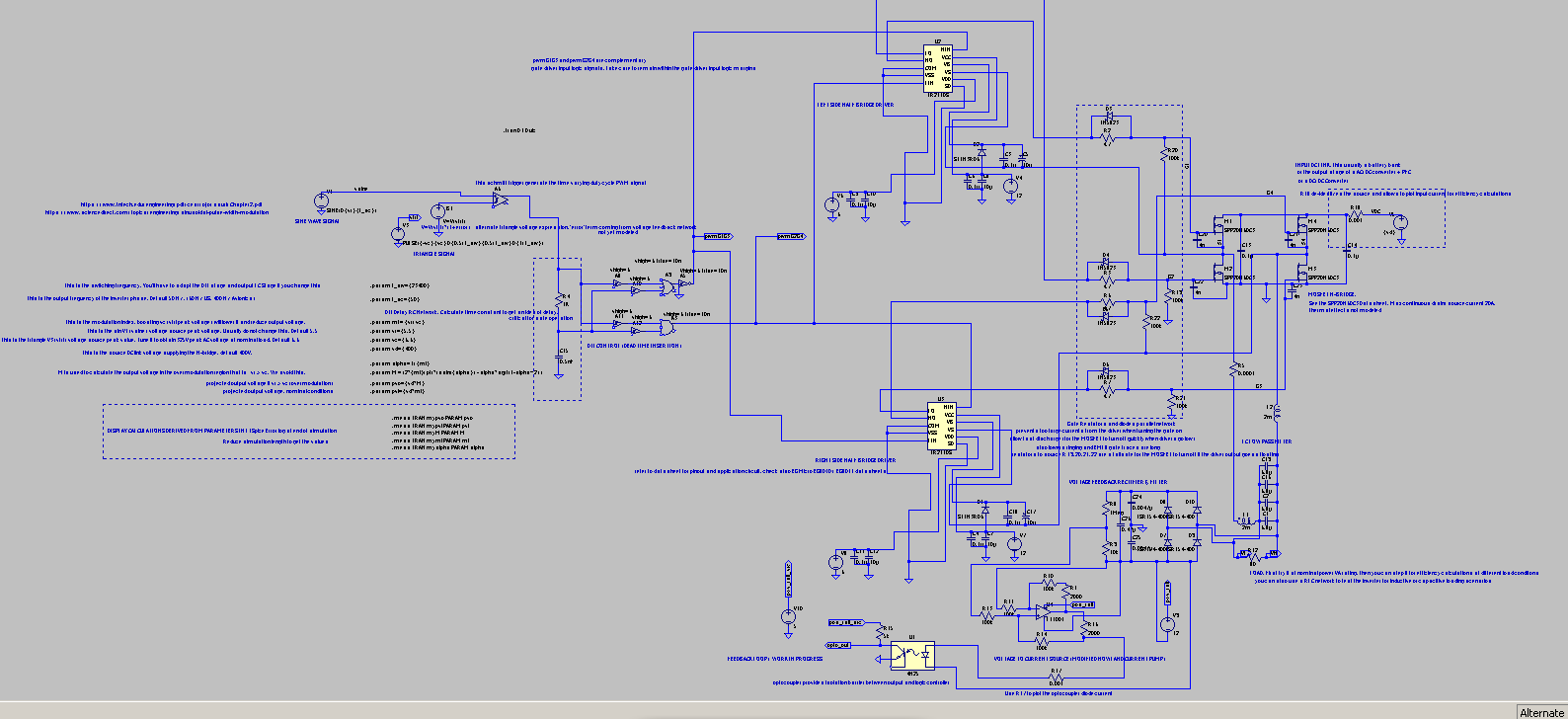
400V DC to 230V AC pure sine wave inverter model using LTSpice.
Note : the above model has been updated for frequency/phase synchronization. please check :
Disclaimer : This design uses dangerous AC and DC voltages. If you get out of the simulation domain and start prototyping be sure to use all safety precautions required when working with high voltages. You have to know what you are doing.

Besides the simulation this post is an introduction on pure sine inverter technology targeted at electronics engineers that have little or moderate experience in power electronics and inverter design.

The goal is to design, implement and prototype your own pure sine wave inverter from scratch as an educational project to get into inverter technology, this will be the object of a series of posts in the future.

For a faster design approach see the bottom of this post on how to use off the shelf inverter modules such as EGS002 or EGS005 available on BangGood and AliExpress.

To get straight into the model simulation go to the running the simulation section.

Introduction

Inverters use MOSFETS to switch a DC source with a variable duty cycle PWM signal.

The duty cycle variation in the time domain is performed at the frequency of the required output fundamental frequency of the inverter.
Usually mains frequency, that is 50hz or 60hz.

The frequency of switching, that is the frequency of the PWM signal is called the switching frequency. it is usually in the 2.5khz to 100khz range.

So, the goal is to have a PWM signal at high frequency (2.5 khz to 100khz) with a variable duty cycle whose frequency is at mains frequency.

However, The variable duty cycle frequency may be lower or higher, or can be adjusted in real time.

Applications that require this duty cycle modulation at fixed but non standard 50Hz or 60hz are mainly for the aerospatial industry.

Airplanes use 400hz. The advantage of 400hz is that power transformers are less bulky than in 50Hz.

There is also an industry need to adjust the inverter output frequency in real time. This is the market segment of VFDs (Variable Frequency Drive) inverters.

This allows to set the rotation speed of induction motors, and allow for a soft-start that does not damage the motor.

In VFD applications, not only the the frequency output of the inverter is managed, but also the output voltage, and sometimes they implement a fixed voltage to frequency ratio mode so the motor stays happy.

So, now comes the question, How to modulate the duty cycle of a PWM signal ?

This is usually done by comparing a triangle signal at the switching frequency with a reference sinusoidal signal at the desired mains frequency.

This can be done in two ways :

1) Using analog components : a sine generator IC (like the XR-2206 or MAX038) that outputs a triangle wave and another one (also XR-2206 or MAX038) that outputs the sine wave. Then, a schmitt trigger is used to compare these two signals to output a PWM signal.

2) Using digital components : the sine modulated variable duty cycle PWM output is generated by code running on MCUs, PIC, DDS IC. Arduino can do this, however Arduino has a limitation that hinders its use for this purpose, and that is dead time control. More on this later.

If you nonetheless want to experiment with SPWM generation with an Arduino, check this code to get an idea of how it works.

I recommend you read resources on Fast PWM for Arduino. It is not straightforward if you have no experience with hardware counters/timers. Check https://www.arxterra.com/tutorial-on-fast-pulse-width-modulation/ and https://docs.arduino.cc/tutorials/generic/secrets-of-arduino-pwm
for starters. You may have to browser for other resources because I could not find one comprehensive documentation for ALL modes, except maybe in AtMel datasheets, but these are very terse and quite hard to understand.

Here is the first code sample :
#include <Arduino.h>

uint16_t freq = 50; // inverter output frequency
uint32_t counter = 0;
uint16_t mod_index = 0.9; // modulation index. you will have to update this in real time for precise voltage control.
float sin_val;
const uint16_t samples_per_period = 100;
// higher samples per period give a better looking output sine wave, less harmonics from digital aliasing
uint16_t micros_interval;

uint16_t sin_table[samples_per_period];

void populate_sin_table()
{

  uint16_t i;
  for(i=0;i<samples_per_period;i++)
  {
      sin_val = 512*(1 + mod_index*sin(2*PI*float(i)/samples_per_period));
      sin_table[i] = round(sin_val);
      //Serial.println(int(sin_val));
  }

}

// FAST PWM PHASE-CORRECT MODE 3

void setup(){

  // Wave Form Generator: phase correct PWM mode 3, Top = OCR1A and OCR1B
  // We will output two signals, complementary, using two pins ~9 and ~10 so we need to specify
  // (0<<COM1A0) + (1<<COM1A1) + (1<<COM1B0) + (1<<COM1B1)
  // (0<<CS10) + (1<<CS11) + (0<<CS12) this is the prescaler and will dictate the switching frequency.
  // (1<<WGM11) + (1<<WGM10); and (0<<WGM13) + (0<<WGM12) are used to set the Fast PWM mode, here we use mode 3.
  // it allows a 10 bit amplitude resolution for the sine wave signal
  // check this link for a table of available modes.


  TCCR1A = (0<<COM1A0) + (1<<COM1A1) + (1<<COM1B0) + (1<<COM1B1) + (1<<WGM11) + (1<<WGM10);
  TCCR1B = (0<<WGM13) + (0<<WGM12) + (0<<CS10) + (1<<CS11) + (0<<CS12);

  OCR1A = 0x3FF; // top compare value initialization. it will be varied using the sine table in the loop.
  OCR1B = 0x3FF; // same for the second PWM signal

  //DDRB |= (1<<PB1);

  //Serial.begin(9600);
  populate_sin_table(); // create a sine table. better use PGM write and store it in flash for a more robust approach
  micros_interval = int(float(1E6)/(float(freq)*float(samples_per_period))); // the loop wait delay between two bit bangings
  // of OCR1A and OCR1B.

  //Serial.println(micros_interval);

}


void loop() {
 delayMicroseconds(micros_interval);
 OCR1A =  sin_table[counter%samples_per_period]; // iterate on the sine table, use modulo to loop the table
 OCR1B =  sin_table[counter%samples_per_period]; // same for the second SPWM

 //Serial.println(sin_table[counter%samples_per_period]);
 //Serial.flush();
 counter++; // overflow not managed !!!!!
}
There is also this wonderful code https://forum.arduino.cc/t/dead-time-between-pwm-signals/937405 for a three phase system. I did not test it but it looks serious and legit. It has the advantage of using ISR and not a loop to update the TOP value with the sine wave, generates 6 signals (so it is for bipolar spwm) but it suffers from the same dead time insertion problem however, and that is the object of the guy’s post. But it is possible with analog post processing, check the DTI section.
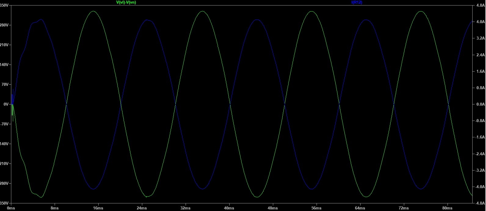
That is why STM32 based boards are better for an all digital SPWM generation purpose, but they are more expensive and you'll need to watch quite a bunch of tutorials to master Nucleo (the STMicroelectronics MCU IDE). It will be easier if you already master Arduino FastPWM generation, but it will require time nevertheless.

Now is a good time to learn about the specifics on how that sine modulated variable duty cycle PWM signal allows the inverter to generate a 50hz, 60hz or higher frequency mains power phase voltage.

The "sine modulated variable duty cycle PWM signal" will be now referred by its usual name in the power electronics technology as SPWM (sine PWM)

The power core : the MOSFET H-bridge

The power core of an inverter uses an H-bridge configuration because the setup of its components ressembles to the letter H.
It is one of the most common designs in the industry.

MOSFETs switch repeateadly a DC source with low source impedance (the power source) according to the input gate signal that comes from the SPWM.

That is not all. high VDS high current MOSFETS usually need gate voltages that are higher than what an MCU or an analog oscillator can generate.
The high side MOSFET gates  of the H-bridge also need voltages with reference to DC ground that are way above the levels of the logic/analog controllers.

For that reason, there is a specific family of ICs that exists and they are called "MOSFET Gate Drivers". Their goal is to bridge the gap between the logic SPWM signals and the required voltage levels (and current requirements) of the MOSFET gates.

Moreover, an H-bridge inverter has at least 4 mosfets. These MOSFETS need to be activated by gate signals at a precise fashion, like a fine tuned choregraphy.

The activation pattern is usually diagonal in the schematics. This has the effect of reversing the polarity with reference to DC GND seen by the load with each pwm pulse. Since the two SPWM signals are complementary in this design, when one diagonal set of MOSFETs has a high duty cycle it will be on and conduct a longer time than the reciprocal diagonal set of MOSFET, when this happens the output sine wave of the inverter is at a +Vo_peak. Then there is a time when the duty cycle 0.5 for both diagonal pairs, at this point the sinusoidal output of the inverter crosses 0V. then the cycle goes in the reverse direction and outout reaches -Vo_peak.


PWM Modulation schemes

I just described one SPWM modulation scheme. There are two schemes that are most commonly used.

- Unipolar SPWM
- Bipolar SPWM

To understand the difference between the two, please read now :

https://www.sciencedirect.com/topics/engineering/sinusoidal-pulse-width-modulation
https://www.tntech.edu/engineering/pdf/cesr/ojo/asuri/Chapter2.pdf

My guide is based on Bipolar SPWM.

As you may already guessed, for that SPWM scheme you need two complementary SPWM signals.
For analog SPWM generation, the original SPWM signal generated from the triangle to sine comparator is fed to a NOT gate to create a complementary SPWM signal.

The original signal will drive the Top Left MOSFET and Bottom Right MOSFET
While the complementary signal will drive the Top Right MSOFET and Bottom Left MOSFET.

Note that in an unipolar SPWM scheme, The complementary SPWM signal stays low the whole time the other one operates, and then starts doing SPWM modulation while the other one stays quiet. This switching happens at 2*f_mains,
I find it harder to generate these two kinds of SPWM signals using digital means, so I think that the bipolar scheme is better to start grasping the technology.

Note also that IC Gate Drivers usually manage two MOSFET for a half bridge configuration. So we need Two gate driver ICs
In the LTSpice model IR2110 is used, as it is quite common in the industry.

The routing between the SPWM signals and gate drivers is as follows in my LTSPICE schematic and simulation :

SPWM signal is provided to HIN input of Gate Driver 1 and LIN of gate Driver 2
Whereas the complementary SPWM signal is provided to LIN input of gate driver 1 and HIN input of gate driver 2

HO output of gate driver 1 drives the top left M1 Mosfet
LO output of gate driver 1 drives the bottom left M2 Mosfet
HO output of gate driver 2 driver the top right M4 Mosfet
LO output of gate driver 2 drives the bottom right M3 Mosfet.

If you connect the dots, you'll see it fits the requirements of bipolar SPWM modulation scheme.

The big issue : dead time control.

There is a factor that needs extra precautions because it can fry the MOSFETs and brick the inverter. In no case, the M1 M2 MOSFETs should conduct at the same time.
This also true for M4 M3. If that would happen, The low impedance DC source will short through these MOSFETs (from Vdc to GND). When driven to high gate voltages, these Power MOSFETs  have a ridiculously low RdsOn, This will generate currents way above the absolute ratings of the MOSFET, frying them if a DC breaker or another protection from the upstream DC link did not catch it in time.

For this reason, a security margin between the two SPWM signals (the original and complementary) has to be put in place, This is a delay between pulses where both SPWM signals remain low. This is called dead time.

a good article to read on that subject :

https://hackaday.io/project/3176-gator-quad/log/11741-pwm-control-and-dead-time-insertion

For digital SPWM generation, forget about Arduino to get SPWM plus dead time control using Phase correct PWM out of the box.
Better PICs or MCUs are required such as STM32.

It is however possible to apply analog treatment to a single SPWM arduino generated signal, to create a complementary signal with a dead time delay inserted before the rising edge and after the falling edge.

In the supplied schematic, it is done through a RC network whose time constant is matched to introduce the required dead time, plus a bunch of gates and schmitt triggers. This setup may be simplified, if you manage to use less components or update the model to use real world components instead of ideal ones, let me know through the contact form.

Output Voltage control and regulation.

Output voltage control of the power stage is performed basically by varying the triangle peak voltage, while the sine voltage remains the same.

The peak output voltage is roughly given by
Vo_peak = V(dc)*V(sine)/V(tri)
Vo_RMS is then V(dc)*(V(sine)/V(tri))/sqrt(2)
V(sine)/V(tri) is known as the modulation index (mi)
it is usually < 1

If V(sine) gets larger than V(tri), the inverter operates in the overmodulating region, and RMS output voltage is no longer linearly dependent on V(dc)
It appears in the simulation as a voltage saturation of the output.

overmodulation is outside the scope of this guide but it is explained in the above mentioned resources.

An open loop control is not realistic because of deviations from theory that assumes ideal components, and dependance on the load RLC parameters and the output filter parameters, as well of the transformer if an isolated output is required.

So there is a need for a voltage feedback loop to the SPWM generating component to adjust the modulation index.

Passing the voltage information to the source controller has to be done properly.

Because of voltage shifts of the (V(l) - V(n)) voltage relative to DC GND even after passing a voltage divider in this unisolated design, galvanic isolation is required, and this is a safety requirement.
If the output is isolated using a mains frequency transformer, galvanic isolation in the feedback loop is inevitable.

There are three methods to create an insulated voltage feedback loop.

- Using an auxilliary winding in the secondary of a mains transformer.
With a turns ratio tuned for low output voltages, usually such as 3.3V/2 (rms) or 5V/2 (rms) is obtained when the inverter output voltage is at nominal conditions. That gives ample room for the signal to go higher if the output stage encounters an overvoltage situation.
One leg would be connected to DC GND, the other fed to a full bridge rectifier, smoothed, and then that voltage would be fed to an error amplifier op-amp (a difference amplifier) that compares it to a precise voltage reference. This difference signal is a negative feedback that is then used to adjust the modulation index if using full analog generation. That would happen by controlling the AM pin of the XR-2206 Triangle generator, for instance.

If the SPWM is generated with digital means, the error amplifier could not even be required.
A DAC may be enough to acquire the voltage output of the optocoupler and the comparison of the DAC output would be done against a digital reference. Then, a digital control method should be implemented to control the feedback loop (such as PID) and update the modulation index.

I digress. Back to the feedback isolation.

- The other way of isolation is to use a separate low power transformer, with it's primary legs in parallel with the load. That is useful if your design does not use a transformer at all for the power stage, so you need only a transformer for feedback. Also, transformers with auxiliary windings are specific and you may have one on hand without that feature.
Of course it should be designed for 50Hz, or 60Hz, or more depending on your output frequency, with a ratio adjusted the same way as for an auxiliary winding.


- The third method involves a rectifier, a smoothing capacitor/filter stage, a voltage divider, which output drives a voltage controlled current source.
In this design I am trying a modified Howland current pump.
This current source is required because it will drive an optocoupler to transmit the analog information across the insulation barrier.
Optocouplers are current driven.

Care has to be taken to operate the optocoupler in its region where the CTR (current transfer ratio) is linear, by setting properly the current source gain.
Then one has to chose the proper collector resistor on the output side of the optocoupler to obtain proper transfer characteristics.

It is advised to test the transfer characteristics of the Current source + Optocoupler in a separate circuit to tune it up before adding it to the design, it will make things faster to simulate and way easier.

The rest of signal processing is the same as with the transformer approach.
Either digital control if SPWM is generated through a MCU or analog if using an oscillator. Analog will need a compensation network (usually a R+C // C) network for the feedback control loop to be stable.

Note : I have yet to model this part in the supplied model. It will be the object of this post revision in the future.

However, the fact that we are dealing with an inverter and that we have to perform rectification and smoothing to extract the peak voltage information, introduces feedback charateristics that are a bit different than DC/DC converter feedback loops.

Since the feedback loop would be designed with non-monolithic components (By that I mean the that the feedback loop does not use complex IC whose internals are a black box if their full transfer characteristics are not provided in the datasheet, and that perform mysteriously during AC analysis), it is possible to perform an AC open loop frequency response analysis of the rectifier + smoothing capacitor + current source + optocoupler quite easily.

Then add and tune a proper compensation network to obtain stability.

Check this guide for an introduction on compensation networks. It is targeted for SMPS power supplies, but the core concepts are the same, that is the need to model the open feedback loop at steady state, introduce a perturbation, and perform an AC analysis to get the frequency and phase response. (The bode plot)

https://www.ti.com/seclit/ml/slup340/slup340.pdf


The LC output filter.

A LC filter is a second order passive filter.
It's goal is to filter the high frequency switching pulses to obtain a pure sine wave with the least amount of harmonics.
In that design, I set the fc (corner frequency) at 10 times the mains frequency, that is 500Hz, not that the lower this frequency, the larger the L and C values, and the larger the effects on voltage with changing load impedannce.

You will notice also that the sine waveform THD will change with loading, appearing less distorted at higher loads

Finally, the LC output stage has an effect on output power factor. An inverter designed for inductive loads will be tuned differently in that regard.

Loading of the filter also affects its response and hence change the output voltage.

Check this thread for a discussion on inverter LC filters :

https://www.edaboard.com/threads/true-sinewave-inverter-output-lc-filter-design-help-needed.375327/

Running the simulation.

Download the zip file in the post introduction. Check the readme.txt in the zip for important information about LTspice setup for that model. Most of the important parameters are parametrized and explained
Most of the inverter functional blocks have commentaries that complement the information given here.
On a core i5 Elitebook 8440p, using LTspice under Wine on Linux, I get around 6.5us/s simulation speed. Try to get at least two or three output sine periods.
This is a work in progress, it will be updated as I improve the model.

A faster approach.

Fortunately, you don't have to reinvent the wheel if you have no time to learn all the intricacies of inverter technology, It is however always better to have an understanding of how all the inverter components work before using a board that implements some of the inverter functions in their design.

For this, there are inverter boards, and we'll have to turn to China and EGMICRO
EGMICRO is a supplier of ASIC inverter boards and more that take care of the SPWM thing, DTI, Gate driving, frequency settings, and voltage feedback, plus they have a monitoring output. They can be used for UPS inverters and also for VFD operation. They also have 3 phase boards.

For single phase designs, there are three ASIC demo boards sold on the market :
- EGS002 is an older but still popular demo board that features the EG8010 ASIC and two IR2110S gate drivers.
I used the same gate drivers in my LTSpice model.
- EGS005 is an newer demo board that features the EG8025 ASIC. It is a monolithic design with integrated gate drivers.

- EGS003 is a board available on the market, with a EG8011 ASIC, plus a single EG2126 package housing a full bridge Gate Driver. But It was since discontinued (the EGMicro website purged the documentation about EG8011) It may have been superseded by EGS005 or it may suffering from issues. Suppliers still sell it. The EG8011 ASIC datasheet still can be found elsewhere. I do not recommend that design if the ASIC supplier made it obsolete.

We will nevertheless perform some intel gathering on these three designs to see how they differ in their reported features.

For three phase designs, There is an EGSO31 board based on the EG8030 ASIC. It uses separate EG3012 gate drivers instead of the more ubiquitous IR2110. A three phase design is necessary for VFD designs powering 3 phase induction AC motors.

To get and idea of how these devices work, you need to check the Demo board, the ASIC and the Gate driver datasheet.
Some of the PDFs are available in simplified Chinese only, but you can pass it to Google translate and have a quite precise idea of what does what after sometimes a little guessing. The quality of Google's technical translations is quite good, since these are terse statements and not litterary works.

The goal is to look precisely at the application schematic and adapt it for our needs.

We will start by investigating the EGS002.

Check that GreatScott's video on EGS002 as an introduction, it also uses a demo UPS board (not just the ASIC+driver board)

https://www.youtube.com/watch?v=Dn2PFebi2ww

Please keep tuned for part II. Where we will discuss EGS002 in more detail to unveil its secrets.
Leave a Reply